Download
1 / 26
360 likes | 854 Views
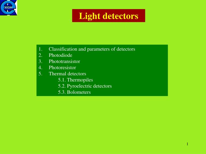
Light detectors. Classification and parameters of detectors Photodiode Phototransistor Photoresistor Thermal detectors 5.1. Thermopiles 5.2. Pyroelectric detectors 5.3. Bolometers. Detectors classification.

E N D
Light detectors • Classification and parameters of detectors • Photodiode • Phototransistor • Photoresistor • Thermal detectors • 5.1. Thermopiles • 5.2. Pyroelectric detectors • 5.3. Bolometers
Detectors classification From the point of view of interaction of electromagnetic radiation with matter, the light detectors can be divided into two major groups: quantumthermal (interaction of photons (variation of detectors parameters with with electrons) temperature due to absorption of radiation) - photovoltaic - thermoelectric - photoconductive - bolometric - photomagnetoelectric - pyroelectric - photoemission Quantum detectors operate from the ultraviolet (UV) to mid infrared (MIR) spectral range. Thermal detectors are used generally in MIR and far infrared (FIR) spectral ranges, where their efficiencies at room temp. are higher than these for quantum detectors.
Detectors parameters Sensitivity (responsivity) It is a ratio of output quantity Y (r.m.s. value of current, voltage) vs. input quantity X (r.m.s. value of radiation power) S = Y/X and accordingly one gets voltage sensitivity SV [V/W], current sensitivity SI [A/W] Sensitivity is a function of wavelength, depending on the detector type. For quantum detectors S initially increases with a wavelength, reaches maximum and then drops to zero at a certain wavelength λC. Sensitivities of quantum detectors are higher than these for thermal detectors and response times are shorter. The advantage of thermal detectors are lower costs and possiblity of work at room temperature. Arrays of thermal detectors are essential part of cheap thermovision cameras. Relative spectral sensitivity of thermal and photonic (quantum) detectors.
Detectors parameters Noise equivalent power (NEP) This is the r.m.s. value of radiation power, which at detectors output gives a signal equal to the noise level, normalised to the unit bandwidth. Commonly one uses the reciprocal quantity – the specific detectivity. Specific detectivity D*(f, λ) (D-star) This is a ratio of signal to noise at unit radiation power, unit sensitive area and unit noise bandwidth. Multiplication by A1/2 comes from the observation that the ratio A1/2/NEP is independent of the detectors sensitive area.
Comparison of detectivities Detectivities in the infrared region of manufactured different detector types (FD - photodiode, FR – photoresistor, TR – thermal detector).
Photodiode A small photocell polarized in a reverse direction is a photodiode. After illumination of the junction the photocarriers generated in a depletion region drift under the influence of junction field enhanced by the external voltage. The carriers generated outside junction within the diffusion length, diffuse in the direction of a junction increasing the current. Photodiode current consists of a dark current depending on the voltage and a photocurrent SΦdepending on illumination S – sensitivity (A/W) Φ – illumination power (W) for U< 0 I= - Is- SΦ - SΦ Ln, Lp – diffusion lengths Wp, Wn – depletion region dp, dn – thickness of p+/n region
Photodiode characteristics Current-voltage characteristics of a photodiode before and after illumination An equivalent circuit of a photodiode: Ip – photoelectric current Id – dark current Rp – leakage (shunt) resistance Rs – series resistance Cp – junction capacitance of a photodiode The electrical bandwidth is determined by Δf = 1/(2πRsCp) and may be improved by reducing Cp with reverse-biased voltage. For a p-i-n photodiode with small Cp,Δfis of order tens GHz.
Structure and working circuits of a photodiode Schottky photodiode On the n- semiconductor (absorption layer) one deposits a thin semitransparent metal layer (Au 10 – 30 nm) and an antireflection coating increasing the transmittance especially in the short-wavelength region. One gets the bandwidth of order 100 GHz. The following semiconductors are often used: Si, GaAs, GaP, GaAsPThe advantage of these photodiodes is their relatively high blue and UV sensitivity. The basic working circuit of a photodiode: uout = RLIp = RLSΦ 0< uout< UB then one obtains a much higher dynamics in comparison to a photocell. A circuit with a photocurrent gain: for R1 = R2 uout = R1I = R1(Ip + Id) hence the dark current is also amplified. This configuration gives however a high bandwidth and dynamics.
Phototransistor It is a light controlled bipolar transistor with internal amplification. In most cases no external connection is made to the base and the base current is supplied by the photogenerated current. Reverse-biased base/collector junction plays the role of a junction photodiode. The light is absobed in a base region. Generated optically current is amplified due to the transistor effect (as explained below). Generated in a base region minority carriers, eg. electrons in an p-type base, diffuse to the collector region increasing its current. Majority carriers in a base region (holes) decrease the potential barrier of the emitter/base junction, increasing at the same time the electron current flowing from the emitter to the base. Electrons in a base are the minority carriers and then are transferred to the collector increasing greatly its current.
Phototransistor IB – optically generated current in a base IE – emitter current αIE – part of emitter current transferred to collector (α<1) α – common base current gain After illumination of the base region one obtains the current (η – quantum efficieny): Photocurrent amplification:
Phototransistor Phototransistors based on Si are readily available at low cost (figure below). fg ~ a few hundred kHz Poor frequency bandwidth arises from the high capacitance of the base-collector junction (τ βRLC) and the long carrier transit times across the base region. However, the high internal gain can greatly simlify detection circuits where the small bandwidth is not a problem (remote control in TV).
Phototransistor The frequency bandwidth can be increased by minimizing the phototransistor dimensions. Heterojunction n-p-n structure of MESA type InP with a higher energy gap plays the role of a window layer and the light is absorbed in a base region. By attaching a lead to the base one removes the carriers from that region what increases the cut-off frequency fg. One reduces at the same time the gain.
Photoresistor Photoresistor with interdigitated electrodes • Thickness of the photosensitive layer should be: • high enough to absorb the incident radiation • low to decrease the dark conductance (low noise). • Thermal Johnson noise is generated by the dark current: Δf – bandwidth, R – resistance, iy – noise current
Photoresistor For photoresistors one can define a quantity being the number of electrons taking part in conductivity, generated by one photon. This is the photoconductivity gain The slow motion of carriers, the holes, will cause the draw of faster electrons, to maintain the charge neutrality condition. This gives the gain of a photocurrent. With the help of mobility μ one can write Inserting numerical data τ = 3 ms, µ = 300 cm2/Vs, L = 0,4 mm, V = 2,4V one obtainsΓ = 450, what makes a photoresistor similar to a photomultiplier). In this way it is beneficial to have small L and at the same time to maintain a high photocurent, the large width of a sample. That is why one uses the interdigitated (comb-like) structure of electrodes. The signal transmission rate is dependent on the element response time bandwidth ~ , then: bandwidth * gain = const ttr – transit time of electrons between electrodes τ – carriers lifetime V- applied voltage, L – distance between electrodes
Photoresistor Dependence of optical absorption coefficient α and photoconductivity σph on the wavelength of absorbed light Decrease of σph in the short wavelength region is caused by absorption in a thin, low conducting layer placed close to the surface. In the long wavelength region photoconductivity disappears due to the decrease of α. This is seen in the variation of sensitivity S(λ) with wavelength.
Photoresistor Semiconductors used for photoresistors manufacturing Eg(eV) AlxGa1-xN 3,4 – 6,2 depending on x CdS 2,4 CdSe 1,8 CdxZn1-xTe dep. on x Si 1,12 Ge 0,67 PbS 0,42 PbSe 0,23 InSb 0,23 Hg1-xCdxTe dep. on x Photoresistor of mercury cadmium telluride working in IR range (2 – 30 μm).
Thermal detectors Thermal detectors are of low manufacturing costs in comparison to photon detectors.The quality of these detectors was greatly improved after introduction of micromachining technology. Recently the uncooled arrays of these detectors working in the IR region (thermovision cameras) are commercially available. The change of detectors temperaturecan be calculated from the heat balance equation (heat consumed and lost in a unit of time are equal to the absobed power) ε – abs. coeff. Cth – heat capacitance Gth – heat conductivity If the incident light varies periodically with time as Φ=Φoexp[jωt], then above equation for the stationary case has the solution: where τth = Cth/Gth is a thermal time constant. Electrical scheme for a thermal detector
Thermocouples The voltage signal of a thermocouple is proportional to the temperature difference of the junctions Therefore voltage sensitivity of a thermocouple, taking into account the calculated ΔT for a thermal detector, is equal The sensitivity increases N times for a series connected N thermocouples, called a thermopile. Taking into accounrt that the basic kind of noise for thermocouples is a Johnson noise, one can write expression for a detectivity as: To obtain a high D* the junction must have small Cth (small time constant), high absorption coef. ε and Seebeck coef. α, small heat conductivity Gth , small electrical resistance R. Spectral sensitivity depends essentially on the transmission of encapsulation window.
Thermopiles A thermopile deposited on the membrane. Two pixels of an array with thermopile structures. SiN absorber, heating the appropriate junction, covers nearly the whole pixel. Thermoelectrodes are made from materials of very high figure of merit. Read-out circuitry is manufactured in a silicon substrate.
Pyroelectric detectors One uses the dependence of spontaneous polarization on temperature for the pyroelectric material and also the dependence of elecrical permittivity on temperature (dielectric bolometer). Spontaneous polarization PS and pyroelectric coefficient p as a function of temperature for a pyroelectric material in vicinity of Curie temperature TC . Electrical permittivity as a function of temperature in vicinity of TC . If the temperature of a dielectric of ferroelectric capacitor changes by ΔT and then polarization by ΔP, the surface charge will be induced with density ΔQ/A and in the external circuit the following current will flow I = dQ/dt = pA d(ΔT)/dt A – dielectric area
Pyroelectric detectors Knowing ΔT from the heat balance solution for periodically changing light intensity, one can determine the current generated by the pyroelectric detector According to the equivalent circuit shown, the voltage generated by the detector is equal and accordingly the voltage sensitivity τe = C/G – electrical time constant Typical values of τth are of order 10 ms, τe can vary in a range 10-12 – 100 s. Pyroelectric detector (shown in a form of an electrical equivalent circuit) at the input of transimpedance amplifier.
Pyroelectric detectors Voltage sensitivity of a pyroelectric detector as a function of frequency. Both electrical and thermal time constants are important. In order to obtain small thermal time constant, pyroelectric detectors are manufactured onto suspended membranes . Bottom electrode and a mirror form a resonant cavity for IR radiation (thickness λ/4). By splitting upper electrode two capacitors are formed, which connected in series enable reducing of noise caused by mechanical vibrations.
Bolometers Bolometer is a resistance element with a high TCR and a small heat capacity. Absorbed infrared radiation changes the temperature and then the resistance of a bolometer. TCR coefficient is defined as: Change of temperature by ΔT causes a change of bolometers resistance by ΔR what gives the output signal Use of high values of R and IB is limited by noise, which in this case are Johnson noise; and 1/f noise: n – 1/f noise parameter Additionally IB is also limited by the maximum working temperature of the sensor.
Metallic and thermistor bolometers Voltage sensitivity of a detector at the sinusoidal variation of incident radiation power can be determined from the dependence as for a thermocouple substituting α by IB a R : Bolometers in a form of thin metallic films (Ni, Bi, Sb) with moderate TCR (typ. 0.3%/K) but high stability and low noise are still manufactured. Thermistor bolometers(Co, Mn, Ni,V oxide sinterings) have one order of magnitude higher TCR but also higher current noise. To increase the detectivity one uses sometimes immersion lenses as radiation concentrators. In this case the signal to noise ratio increases n2 times due to n-th increase of a detector area (n- refractive index of a lens material, eg. Si, Ge). Bolometer in a bridge circuit with compensation of ambient temperature variations Bolometer with immersion lens
Semiconductor and micromachined bolometers High detectivities are obtained by using semiconductor bolometers (Ge, Si) at cryogenic temperatures. At very low temperatures the relative changes of semicondutor resistance are higher and absorbing samples are thicker (lower specific heat) what increases absorption. In a far infrared region these detectors have detectivities comparable to those of photonic detectors, hence their applications in astronomy, spectroscopy etc. Application of micromachining enabled manufacturing of microbolometers with a high thermal resistance (1x 10⁸ K/W), close to the theoretical limit caused by radiation. Bipolar CMOS input amplifiers are used in readout circuits. Double-level 50 x 50 µm2 bolometer manufactured in micromachining technology (Honeywell 1992). Active VOx layer is deposited onto Si3N4 plate supported by two narrow legs over the silicon substrate with integrated readout circuit.
Superconducting bolometers Very high variation of resistance for a small change in temperature is obtained for superconductors in the vicinity of critical temperature Tc. The development of this technology was possible due to the discovery of high temperature semiconductors, HTSC. The typical HTSC material is YbBa2Cu3O7-x (YBaCuO) with transition temp. ca 90 K. Using this material and micromachining technology it was possible to obtain bolometers with detectivities close to 1010 cmHz1/2/W (better than for photonic detectors at 77 K). Variation of resistance in the vicinity of critical temperature Tc. Superconducting microbolometer in micromachining technology