Download
1 / 35
350 likes | 514 Views
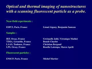
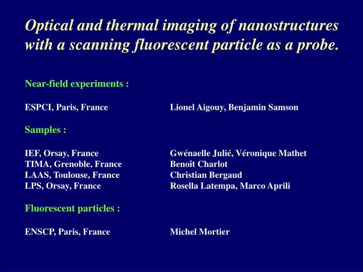
Optical and thermal imaging of nanostructures with a scanning fluorescent particle as a probe. Near-field experiments : ESPCI, Paris, France Lionel Aigouy, Benjamin Samson Samples : IEF, Orsay, France Gwénaelle Julié, Véronique Mathet TIMA, Grenoble, France Benoît Charlot

E N D
Optical and thermal imaging of nanostructures with a scanning fluorescent particle as a probe. • Near-field experiments : • ESPCI, Paris, France Lionel Aigouy, Benjamin Samson • Samples : • IEF, Orsay, France Gwénaelle Julié, Véronique Mathet • TIMA, Grenoble, France Benoît Charlot • LAAS, Toulouse, France Christian Bergaud • LPS, Orsay, France Rosella Latempa, Marco Aprili • Fluorescent particles : • ENSCP, Paris, France Michel Mortier
OUTLINE Introduction : fluorescent particle as a local sensor
OUTLINE Introduction : fluorescent particle as a local sensor A local optical sensor (evanescent fields) Local field around metallic nanoparticles
OUTLINE Introduction : fluorescent particle as a local sensor A local optical sensor (evanescent fields) Local field around metallic nanoparticles Surface plasmons polaritons launched by apertures
OUTLINE Introduction : fluorescent particle as a local sensor A local optical sensor (evanescent fields) Local field around metallic nanoparticles Surface plasmons polaritons launched by apertures A local thermal sensor Hot zones in a polysilicon resistive stripe
OUTLINE Introduction : fluorescent particle as a local sensor A local optical sensor (evanescent fields) Local field around metallic nanoparticles Surface plasmons polaritons launched by apertures A local thermal sensor Hot zones in a polysilicon resistive stripe Heating of an aluminum track
HOW DOES IT WORK ? PM Filters Microscope objective Electromagnetic field on the surface Sample Laser Map of the field distribution on the surface
HOW DOES IT WORK ? PM Filters Many dipoles randomly oriented Microscope objective Electromagnetic field on the surface APL, 83, 147 (2003) Sample Simplicity Detection of the total electromagnetic field on the surface (Ex, Ey, Ez) Laser Map of the total field distribution on the surface
HOW DOES IT WORK ? PM Filters Many dipoles randomly oriented Microscope objective Electromagnetic field on the surface APL, 83, 147 (2003) Sample Simplicity Detection of the total electromagnetic field on the surface (Ex, Ey, Ez) Laser (=974nm) Er / Yb ions Robust : inorganic → no photobleaching Infrared excitation : emission and absorption lines well separated (= 550nm) Non linear excitation : fluo I2→Contrast enhanced
TIP FABRICATION Attachment of the particle Applied Optics, 43(19) 3829 (2004) Optical images : 16.5 x 11.7 mm2
TIP FABRICATION Attachment of the particle Applied Optics, 43(19) 3829 (2004) Optical images : 16.5 x 11.7 mm2 exc = 975 nm Lateral resolution : / 5 200nm size particle
LOCAL OPTICAL FIELDS : NANOPARTICLES Gold and latex particles on a surface AFM Particle diameter : 250 nm
LOCAL OPTICAL FIELDS : NANOPARTICLES Gold and latex particles on a surface AFM Fluorescence Particle diameter : 250 nm
LOCAL OPTICAL FIELDS : NANOPARTICLES Gold and latex particles on a surface AFM Fluorescence Particle diameter : 250 nm Gold Latex Latex Fluorescence is enhanced on gold particles JAP, 97 104322 (2005).
LOCAL OPTICAL FIELDS : NANOPARTICLES Gold and latex particles on a surface AFM Fluorescence Particle diameter : 250 nm Gold Latex Latex Fluorescence is enhanced on gold particles Map of the field distribution on the structure Dark ring around the particle : interference between the incident and the scattered wave. JAP, 97 104322 (2005). Circular symmetry of the field distribution
LOCAL OPTICAL FIELDS : NANOSLIT APERTURES scan TM-polarized excitation SEM 10,44µm
LOCAL OPTICAL FIELDS : NANOSLIT APERTURES d=10,44µm scan TM-polarized excitation SEM 10,44µm
LOCAL OPTICAL FIELDS : NANOSLIT APERTURES d=10,44µm scan TM-polarized excitation Period = 480.5 nm ± 2 nm spp / 2 = 481.6 nm Good agreement with the SPP wavelength
OTHER APPLICATION : TEMPERATURE MEASUREMENTS Fluorescent particle Emission varies with temperature
OTHER APPLICATION : TEMPERATURE MEASUREMENTS Fluorescent particle Emission varies with temperature Tip Laser beam Fluorescent particle Stripe Microelectronic device
OTHER APPLICATION : TEMPERATURE MEASUREMENTS Fluorescent particle Emission varies with temperature Tip Laser beam Fluorescent particle Stripe If we know the temperature dependence of the fluorescence, then we can determine the temperature T ° I Microelectronic device
OTHER APPLICATION : TEMPERATURE MEASUREMENTS Pollock & Hammiche, J. Phys. D 34, R23 (2001) Improvement of the lateral resolution Highly localized sensor
OTHER APPLICATION : TEMPERATURE MEASUREMENTS Pollock & Hammiche, J. Phys. D 34, R23 (2001) Improvement of the lateral resolution Highly localized sensor Low parasitic heating by convection through the air
HOW CAN WE DEDUCE THE TEMPERATURE ? PL spectrum of Er / Yb doped particles Er / Yb ions
HOW CAN WE DEDUCE THE TEMPERATURE ? PL spectrum of Er / Yb doped particles Er / Yb ions 4F7/2 2H11/2 4S3/2 (980 nm) (527 nm) (550 nm) (980 nm) 4I15/2
EXPERIMENTAL SET-UP Topography Oscillating tip Microelectronic circuit Tapping mode (f=6kHz, amplitude=10nm) Scanning stage
EXPERIMENTAL SET-UP Laser beam (980nm) Topography F=620Hz Oscillating tip Microelectronic circuit Tapping mode (f=6kHz, amplitude=10nm) Scanning stage
EXPERIMENTAL SET-UP Laser beam (980nm) Beam splitter Topography F=620Hz Oscillating tip Microelectronic circuit Tapping mode (f=6kHz, amplitude=10nm) Scanning stage
EXPERIMENTAL SET-UP Laser beam (980nm) Optical image 1 PMT Lock-in 520nm Filter Beam splitter Topography F=620Hz Oscillating tip Microelectronic circuit Tapping mode (f=6kHz, amplitude=10nm) Scanning stage
EXPERIMENTAL SET-UP Laser beam (980nm) Optical image 1 PMT Lock-in 520nm Filter 550nm Beam splitter Lock-in PMT Filter Topography F=620Hz Oscillating tip Microelectronic circuit Tapping mode (f=6kHz, amplitude=10nm) Scanning stage Optical image 2
DOES THAT WORK ? Collaboration : B. Charlot (TIMA, Grenoble), G. Tessier (ESPCI, Paris) Microelectronic device : Polysilicon resistor stripe (covered with SiO2 and Si3N4 layers) Topography Yellow optical image (550nm) Green optical image (520nm)
DOES THAT WORK ? First experiment : no current circulating in the resistor Yellow fluorescence image (550nm) Green fluorescence image (520nm) Topography Scan size : 45µm x 60µm
DOES THAT WORK ? First experiment : no current circulating in the resistor Yellow fluorescence image (550nm) Green fluorescence image (520nm) Topography I = 0 mA Uniform temperature (room temperature) Optical contrast visible between different zones Reference image Scan size : 45µm x 60µm
DOES THAT WORK ? Second experiment : a current circulates in the resistor I = 50 mA Hot spots I = 0 mA Uniform temperature (room temperature) Optical contrast visible between different zones Reference image APL, 87, 184105 (2005).
CONCLUSION Scanning near-field fluorescent probes have really interesting imaging capabilities ! • Nano-optics : evanescent fields (localized, surface plasmons polaritons) • Nano-thermics : heating in stripes, failure analysis, … UNIVERSAL DETECTOR ! Future : - Reduce the size of the fluorescent particle : to get a better resolution - Many studies : plasmonics and thermics Acknowledgments : Philippe Lalanne (Institute of Optics, Orsay, and US Dax supporter)