Download
1 / 21
220 likes | 528 Views
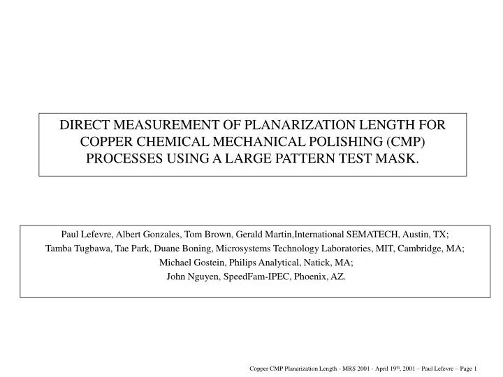
DIRECT MEASUREMENT OF PLANARIZATION LENGTH FOR COPPER CHEMICAL MECHANICAL POLISHING (CMP) PROCESSES USING A LARGE PATTERN TEST MASK. Paul Lefevre, Albert Gonzales, Tom Brown, Gerald Martin,International SEMATECH, Austin, TX;

E N D
DIRECT MEASUREMENT OF PLANARIZATION LENGTH FOR COPPER CHEMICAL MECHANICAL POLISHING (CMP) PROCESSES USING A LARGE PATTERN TEST MASK. Paul Lefevre, Albert Gonzales, Tom Brown, Gerald Martin,International SEMATECH, Austin, TX; Tamba Tugbawa, Tae Park, Duane Boning, Microsystems Technology Laboratories, MIT, Cambridge, MA; Michael Gostein, Philips Analytical, Natick, MA; John Nguyen, SpeedFam-IPEC, Phoenix, AZ.
Introduction Pre CMP topography International Sematech / MIT Mask 862 design Wafer process and metrology Planarization Length definition Planarization Length on different process Planarization Length on different consumables Conclusion Agenda
Visual observation copper residue are more or less pattern dependent (Qualitative) Feature size design / Pre CMP topography size Develop a direct qualitative method for planarization distance measurement. Help industry with having access to this mask International Sematech / MIT 862 (Semiconductor and CMP suppliers) Introduction
Pre CMP topography 50 um copper line, 50 um space 0.25 um copper line, 0.25 um space 1 um copper line, 1 um space 9 um copper line, 1 um space
Small structures Small features (5mm x 4mm)
Wafer process Copper Thickness is 2X trench height
Metrology • Measurements • performed on • Philips Impulse 300 • 15 measures per • Structure • 5 left • 5 center • 5 right
Results PE = 1 – Bottom / Top Top - Bottom
Results Log Scale Minimum Planarization Length Maximum Planarization Length Average planarization Length
Average planarization Length = (Min PL) x (Max PL) Planarization LengthsAverage Planarization Length Maximum Planarization Length = Minimum Feature size were removal bottom equal removal top Or Maximum Planarization Length = Minimum Feature size were planarization Efficiency is zero Minimum Planarization Length = Maximum Feature size where removal bottom is zero Or Minimum Planarization Length = Maximum Feature size where planarization efficiency is 1 Average Planarization Length on a Log scale diagram is = Exp ( Average (Min PL, Max PL))
Process comparison Low Planarization Length Very high Planarization Length
New International Sematech / MIT mask 862 allow a direct measure of planarization Length Definition of Planarization Length Wafers mask 862 available – In public domain Conclusion