Download
1 / 9
90 likes | 345 Views
Computational Nano-Electronics Initiative (CNEI) (http://www.ntu.edu.sg/eee/eee6/CNEI/). Computational Nano-Electronics Group ( CNEG) Staff: Ast/P Ang Lay Kee, Ricky Ast/P Sun Chang Qing A/P Au Yeung Tin Cheung Ast/P Yu Siu Fung Ast/P Chen Tupei A/P Zhou Xing

E N D
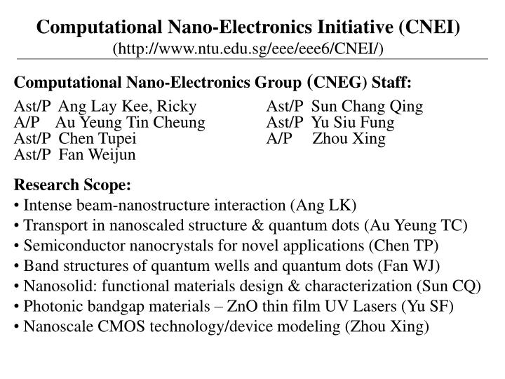
Computational Nano-Electronics Initiative (CNEI) (http://www.ntu.edu.sg/eee/eee6/CNEI/) • Computational Nano-Electronics Group (CNEG) Staff: • Ast/P Ang Lay Kee, Ricky Ast/P Sun Chang Qing • A/P Au Yeung Tin Cheung Ast/P Yu Siu Fung • Ast/P Chen Tupei A/P Zhou Xing • Ast/P Fan Weijun • Research Scope: • Intense beam-nanostructure interaction (Ang LK) • Transport in nanoscaled structure & quantum dots (Au Yeung TC) • Semiconductor nanocrystals for novel applications (Chen TP) • Band structures of quantum wells and quantum dots (Fan WJ) • Nanosolid: functional materials design & characterization (Sun CQ) • Photonic bandgap materials – ZnO thin film UV Lasers (Yu SF) • Nanoscale CMOS technology/device modeling (Zhou Xing)
Research Activities • Call for a Temasek Professor (lead by A/P Zhou Xing): • CNEI co-initiated with IHPC • In the process of searching for a TP candidate • Research Projects / Manpower: • A total of 9 funded projects whose PI or Co-PI are CNEG staff • Funding sources: A*STAR, AcRF, NTU, and CSM • Manpower:1 RF, 11 PhD students and 2 MEng students • Research Collaboration: • Local: IHPC, NUS, and CSM • Oversea: U. Hong Kong, LSI Logic, U. Michigan, and • Los Alamos Nat. Lab.
Interaction of intense electron beam with nano-structures (by Ast/P Ang Lay Kee) • Fundamental Understanding (Theory): • Beam limiting current and beam stability • Beam loading and beam modulation • Coupling between beam and input signal • Detune and de-Q of nano-cavity • Applications of the theory/model: • Simulation of field emitter array of nanotubes or nanotips • Design of high-power, high-freq vacuum micro- & nano-devices • Simulation Code Development: • Including quantum effects in typical PlC simulation codes • Facilities: • 3 PIC simulation tools: PDP1D, OOPIC2D and MAGIC3D
Transport in nanoscaled structure & quantum dots (by A/P Au Yeung Tin Cheung) • The effect of contacts on the ac transport in nanoscaled double-barrier resonant tunnelling structure: • Calculation of the scattering matrix and density ofstates. • Calculation of the ac conductance in the system. • Investigation of the effect of contact on the ac transport. • The ac transport in coupled quantum dot system in the presence of coulombinteractions between the tunnelling and inter-dot capacitances: • Investigate the gauge invariance of potential in the presence of coulomb interactions between tunnelling and inter-dot capacitances. • Calculation of the ac conductance in the presence of the coulomb interactionsbetween various capacitances. • Investigation of the effect of the coulomb interactions between various capacitanceson the ac transport in tunnelling-coupled quantum dot systems.
Semiconductor nanocrystals for novel applications (by Ast/P Chen Tupei) • Potential applications of semiconductor nanocrystals (nc): • Silicon-based optoelectronics: • Strong room-temperature light emission of semiconductor nc embedded in SiO2 thin filmsprovides the possibility of integration of optoelectronic devices into Si circuits with mainstream CMOS process. • Single electron devices: • Coulomb blockade effect of semiconductor nc provides the possibility of single electron devices such as single electron memory cells and single electron transistors (SETs) operating at room temperature. • Research directions: • Theoretical and experimental studies of size effect on physical properties • Calculations of electronic structures of nc and nc/SiO2 interface
Band structures of quantum wells and quantum dots (by Ast/P Fan Weijun) • The 66 k.p effective mass theory for QWs • Band structures of Ga1-xInxNyAs1-y/GaAs compressively strained QWs • The squared optical transition matrix elements • The DOS of Ga1-xInxNyAs1-y/GaAs QWs • The 66 k.p effective mass theory for QDs • Band structures of InAs/GaAs and InGaAs/GaAs QDs
Nanosolid: functional materials design and characterization (by Ast/P Sun CQ) Modeling calculation Shape and size dependency Catalytic effect Self-assembly and thermal stability Room temperature super-plasticity Design and fabrication Photonics and dielectrics of passivated p-Si Ferromagnetic nitride nano-films Oxide photonic crystal and photoluminescence Characterization Bond order-length-strength correlation Single atomic bond and energy levels of an isolated atom
…. …. Investigation of Novel Photonic Bandgap Materials – ZnO Thin Film UV Lasers (application) (by Ast/P Yu Siu Fung) fine hexagonal grain structure Experiments Periodic hexagonal grain forms a 2D periodic structure – can be fabricate by FCVA in our IBP lab ZnO thin film ZnO thin film with hexagonal grains • Current Research/Investigation • - Design ZnO thin film with hexagonal grain structure as a high • power and high efficiency UV laser cavity. • Optimization of grain size and study the influence on the non-ideal • periodic distribution of the hexagonal grains.
Nanoscale CMOS Technology/Device Modeling (by A/P Zhou Xing) • Compact model for nanoscale CMOS technologies: • Physics-based compact model (CM) (DC/AC/RF) for circuit simulation with geometry/bias/temperature scalability and predictability, characterized from given technology data • Numerical modeling and simulation of deep-submicron processes and devices: • Understanding of novel device structures and process effects • Guidance to technology developers and feedback to CM development • Hierarchical modeling at the circuit/gate/block level: • “Seamless integration of simulation modules with focus on the interplay and interfacing of the modules in order to enhance design effectiveness” [ITRS2001: difficult challenge beyond 2007 in complementing continuum tools with atomic ones] • Facilities: Complete suite of Synopsys (TMA) TCAD tools