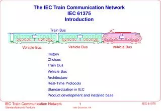
Download
1 / 21
210 likes | 335 Views
ARCHITECTURE. The architecture of SAP-1 shows that it is a bus-organized computer.All register outputs to the W bus are three-state;this allows orderly transfer of data. The program is stored at the beginning of the memory with the first instruction at. Program Counter:

E N D
ARCHITECTURE The architecture of SAP-1 shows that it is a bus-organized computer.All register outputs to the W bus are three-state;this allows orderly transfer of data. The program is stored at the beginning of the memory with the first instruction at
Program Counter: • The program is stored at the beginning of the memory with the first instruction at binary address 0000,the second at 0001 and so on. The PC is a part of the control unit. Its job is to send to the memory the address of The address of the next instruction to be executed and fetched. Process: 1)The pc is reset to 0000 before each computer run
2)When the computer run begins,the pc sends address 0000 to the memory. 3)The pc is then incremented to get 0001. 4)After the first instruction is fetched and executed,the pc sends address 0001 to the memory. 5)Again the pc is incremented. 6)After the second instruction is fetched and executed,the pc sends address 0010 to the memory. In this way, the pc is keeping track of the next instruction to be executed.
Input and Mar: • 1)The memory address register(MAR) is latched with the address of the pc during a computer run. • 2)A bit later,the MAR applies this 4-bit address to the RAM,where a real read operation is performed. • 3)It has some switch registers which helps it to do so. • RAM: • 1)The RAM is a 16x8 static TTL RAM. • 2)During a computer run,the RAM receives 4-bit addresses from the MAR and a READ operation is performed. In this way,the instruction or data word stored in the RAM is placed on the W-bus.
Instruction Register: 1)The instruction register is part of the control unit. 2)To fetch an instruction from the memory the computer does a memory read operation.This places the contents of the addressed memory location on the W-bus. 3)At the same time,the IR is set up for loading on the next positive clock edge. 4)The contents of the IR are split into two nibbles. 5)The upper nibble is a two state output that goes directly to the block labled ‘Controller-sequencer’. 6)The lower nibble is a three state output that is read onto the W-bus when needed.
Controller-Sequencer 1)Before each computer run,(CLR)¯ signal is sent to the pc and CLR signal to the IR. 2)This resets the pc to 0000 and wipes out the last instruction in the IR. 3)A clock signal CLKis sent to all buffer registers,this synchrinizes the operation of the computer. 4)The 12 bits that come out of the CS form a word controlling the rest of the computer.The 12 wires carrying the control ord are called the control bus. 5)The control word has the format: --- --- --- --- --- --- --- CON=CP EP LM CE L1 E1 LA EA SU EU LB LO
This word determines how the registers will react to the next positive CLK edge. • Accumulator: • 1)The accumulator is a buffer register that stores immediate answers during a computer run. • 2)It has two output.The first one goes directly to the adder-subtractor. • 3)The three state output goes to the W-bus when EA is high. Adder-Substractor: 1)When SU is low,the sum out of the adder-substractor is S=A+B When SU is high,the sum out of the adder-substractor is --- S=A+B
3)The adder-substractor is asynchronous (unlocked);this means that its contents can change as soon as the input words change. • 4)When EU is high,these contents appear on the W-bus. • B Register: • The B register is also a buffer register. • A low LB` and positive CLK edge load the word on the W-bus into the B-register. 3)The two state output of the B register drives the B- register. Output Register: 1)At the end of a computer run,the accumulator contains the answer to the problem being solved.At this point,we need to transfer the answer to the outside world.This is where the output register is used.
3)When EA is high, LO` is low,the next positive clock edge loads the word of the accumulator into the output register. 4)The output register is often called an output port processed data can leave the computer through these register. Output Port: 1)The binary display is a row of 8 LEDs . 2)Each LED connects to one flip-flop of the output port. 3)After we have transferred an answer from the accumulator to the output port,we can see the answer in binary form. INSRUCTION SET: LDA: 1)LDA stands for “load the accumulator”. 2)A complete LDA instruction includes the hexadecimal address of the data to be loaded.
ADD: 1)A complete ADD instruction includes the address of the word to be added. 2)For onstance,ADD 9H means ‘add the contents of memory location 9H to the accumulator contents’. 3)The sum replaces the original contents of the accumulator. SUB: 1)A complete SUB instruction includes the address of the word to be subtracted. 2)SUB CH means ‘subtract the contents of the memory location CH from the contents of the accumulator.
3) The difference out of the adder-substractor then replaces the original contents of the accumulator. OUT: 1)The instruction OUT tells the SAP-1 computer to transfer the accumulator contents to the output port. 2)After OUT has been executed,we can see the answer to the poblem being solved. HLT: 1)HLT stand for halt. 2)This instruction tells the computer to stop processing 3)HLT is complete by itself,we do not need to use RAM word using HLT because it does not involve memory. Memory Reference Instruction: • LDA,ADD,SUB
2) They use data stored in the memory. Non Memory Reference Instruction: • OUT,HLT 2) They use data stored in the memory. Mnemonics: Abbreviated instructions like LDA, ADD, SUB, OUT, HLT are called mnemonics. PROGRAMMING SAP-1: 1)To load instruction and data words into the SAP-1 memory,we have to use some kind of code that the computer can interpret.
2)Any program like the forgoing is saidto be written in machine language.It is called object program. 3)The program written in mnemonics is said to be written assembly language.It is called the source program. 4)sometimes we refer to the MSBs of the instructions as instruction field and to the LSBs as the address field. FETCH CYCLE: 1)The control unit is the key to a computer’s automatic operation. 2)The CU generates the control words that fetch and execute each instruction. 3)While each instruction is fetched and executed,the computer passes through different timing states(T states),periods during which register contents change.
The Sap-1 Microprogram • Microinstructions • The controller-sequence sends out control words,one during each T- state or clock cycle.These words are like directions telling the rest of the computer what to do.Because it produces a small step in the data processing,each control word is called a microinstruction. • Macroinstruction • The instructions LDA,ADD,SUB are sometimes called macroinstructions.Each Sap-1 macroinstruction is made up of three microinstructions. • Simplified ,hexadecimal form has also been included.
The Sap-1 Schematic Diagram • Control Matrix • The LDA,ADD,SUB and OUT signals from the instruction decoder drive the control matrix,C39 to C48. • At the sme time,the ring counter signals,T1 to T6,are driving the matrix(a circuit receiving two groups of bits from different sources). • The matrix produces CON,a 12-bit microinstruction that tells the rest of the computer what to do.
Microprogramming • The control matrix is one way to generate the microinstructions needed for each execution cycle.With larger instruction sets,the control matrix becomes very complicated and requires hundreds or even thousands of gates. • Microprogramming is the alternative.The basic idea is to store microinstructions in a ROM rather than produce them with a control matrix. • This approach simplifies the problem of building a controller-sequencer.
Storing the Microprogram • By assigning addresses and including the fetch routine,we can come up with the Sap-1microinstructions .These microinstructions can be stored control ROM with the fetch routine at addresses at 0H to 2H,the LDA routine at addresses 3H to 5H,the ADD routine at 6H to 8H. • To access any routine,we need to supply the correct addresses.For instance,to get the ADD routine,we need to supply addresses 6H,7H and 8H.To get the OUT routine,we supply addresses CH,DH,EH.Therefore,accessing any routine requires three steps: • 1.Knowing the starting address of the routine • 2.Stepping through the routine addrersses • 3.Applying the addresses to the control ROM.
Address ROM • The address ROM contains the starting addresses.The starting address of the LDA routine is 0011,the starting address of the ADD routine is 0110 and so on. • When the op-code bits I7I6I5I4 drive the address ROM,the starting address is generated.For instance,if the ADD instruction is being executed, I7I6I5I4 is 0001.This is the input to the address ROM,the output of the ROM is 0110. • Presettable Counter When I3 is high,the load input of the presettable counter is high and the counter loads the starting address from the addressROM.During the other T states,the counter counts.
Initially,a high CLR signal from the clear-start debouncer is differentiated to get a narrow spike.This resets the counter. • The op code in the IR controls the execution cycle.If an ADD instruction has been fetched,the I7I6I5I4 bits are 0001. • These opcode bits drive the address ROM,producing an output of 0110.This starting address is the input to the presettable counter. • When T3 is high,the negative clock edge loads 0110 into • the presettable counter.The counter is now preset,and counting can resume at the starting address of the ADD routine. • Control ROM • The control ROM stores the SAP-1 microinstructions .During the fetch cycle,it receives addresses 0000,0001,0010.Therefore its outputs are
5E3H • BE3H • 263H
Variable Machine Cycle The microinstructions 3E3H is a NOP.It occurs once in the LDA routine and twice in the OUT routine.These NOPs are used in SAP-1 to get a fixed machine cycle. In some computers a fixed machine cycle is an advantage. But when speed is important,the nops are a waste of time and can be eliminated. One way to do so is by redesigning the circuit to reduce the T-states.