Download
1 / 173
1.82k likes | 2.8k Views
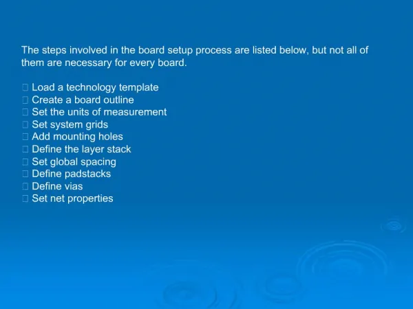
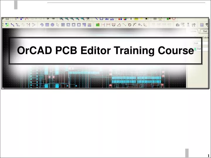
OrCAD PCB Editor Training Course. AGENDA. Lesson 1 OrCAD PCB Editor User Interface Lesson 2 Managing the PCB Editor Work Environment Lesson 3 Component Symbols Lesson 4 Board Design Files Lesson 5 Setting Design Constraints

E N D
AGENDA • Lesson 1 OrCAD PCB Editor User Interface • Lesson 2Managing the PCB Editor Work • Environment • Lesson 3 Component Symbols • Lesson 4 Board Design Files • Lesson 5 Setting Design Constraints • Lesson 6 Preparing for Post Processing • Lesson 7 Preparing the Board Design for • Manufacturing
Lesson 1: OrCAD PCB Editor User Interface Learning Objectives • Identify the user interface components of OrCAD PCB Editor • Navigate within the PCB Editor window and access UI features to tailor the tool to your individual needs
OrCAD PCB Editor and Workspace Title Bar Menu Bar Icons/ toolbars route tool set shape tool set Design Window Status Window Console Window
Toolbar • Toolbars are used to store common icons in a group • Toolbars can be added, modified, or made invisible by using the View > Customization >Toolbar command File Edit Undo/Redo View Add Display Setup Place Shape Manufacture Route Dimension
Control Panel and World View Window • Options Folder Tab • Displays current parameters and values for the active command • Contains fields that let you control the actions performed by the current command • Find Folder Tab (Find Filter) • Controls which objects are found when directly selecting objects • Can also select objects by entering their name • Visibility Folder Tab • Controls visibility/invisibility of conductor/etch elements in the design • World View Window • Allows you to display a particular section of your design • Displays the current viewing area relative to entire design
Navigating using the World View Window Highlighted component Right mouse button popup Whole design Current display window Board outline
Mouse Buttons • Three-button mouse • Left mouse button (LMB)— Select design elements, menu buttons and icons. Window selection available by dragging • Right mouse button (RMB)—Open pop-up menus • Middle mouse button (MMB)—Pan, zoom control
Running Commands with Strokes Tools > Utilities > Stroke Editor
Stroke 명령의 실행 Setup > User Preferences…
Controlling the Toolbars View > Customization > Toolbar
Drawing Options: Display and Status Plated Holes Filled Unfilled Setup > Drawing Options Jogged Report is generated Straight
Drawing Options: Line Lock and Symbol Setup > Drawing options Line 90 45 Arc Off
User Preferences Setup > User Preferences • Can be effective: • Immediate • Restart • Repaint • Next Command Brief description of variable
Lesson 2: Managing the OrCAD PCB Editor Work Environment Learning Objectives Control the color and visibility of objects. Create and use scripts. Use the Control Panel to locate board database objects and report information about them.
Class - 설계상에 표시되는 모든 타입의 아이템
Options Window of the Control Panel Edit > Change Route > Connect Add > Text
Controlling Color and Visibility or... Display > Color/Visibility All On or All Off Select a Group Groups Classes Subclasses Read/write palette settings Custom color blending
Controlling Etch Visibility Include Plane Layers Color View Conductor layer controls Plane layer controls Individual layer controls Individual element control
Graphics Dimming or Shadow Mode Toggles on/off Shadow Mode
Color Priority Display > Color Priority
The Selectable Objects List • You use the Design Object Find Filter section of the Find folder tab when selecting data base elements with the mouse. • The “list” is searched for items that are checked ALONG with the color priority. • The “type” that is found with the highest color priority and a check will be used for the selection. • If there is only one item found at the selection point, the first check box found when searched from top left to bottom right will be used. Challenge: Given the settings to the right, when the Delete command is executed, what will be selected for deletion in the following two scenarios (note the cursor location)?
Using the Find by Name Section • Use the Find by Name section of the Find Folder tab to: • Highlight a net name. • Locate a part placed in the design by its ref. des. 1 Use the pull-down field to set which type of a name you will enter. 2a Enter the name in the blank (>) field. 2b Use the More button to display a scrollable list of all elements matching the desired “type.” • NOTE: The check boxes selected in the Design Object Find Filter have no affect when using the Find by Name section, with the exception of the Property pull-down field. 1 2a 2b
Using Find by Property Use the Find by Property option to select database elements with a common property such as “FIXED”, “MIN_LINE_WIDTH”, and so forth. 3 1 2
Highlighting Elements Display > Highlight Common sequence for highlighting elements with the mouse is: …or 1 Start the command. 2 Activate the Find Folder tab. 3 Click the All Off button. 4 Toggle on desired elements. 5Select the elements in the design window to highlight.
Using the Show Element Command Common sequence for using Show Element with the mouse is: Display > Element …or 1 Start the command. 2 Activate the Find folder tab. 3Click the All Off button. 4Toggle on desired elements. 5Select the elements in the design window.
Using the Display Measure Command Display > Measure …or Verify the settings in both the Find Folder tab and the Options Folder tab Bottom Pin If the class and subclass settings are incorrect, the Display Measure command may not return the desired results.
Lesson 3: Padstacks • Learning Objectives • Create a flash symbol used for thermal reliefs • Use the Pad Designerto create padstacks for a number of typical pins, such as through-hole and surface-mount pads
Anatomy of a Padstack mask Surface-Mount Padstack Through-Hole Padstack top paste mask inner top anti - pad thermal relief inner bottom mask drill size
Padstack Details regular TR_80_60 anti-pad • Regular Pad:A positive pad with a regular shape (circle, square, rectangle, oblong). Flashed on positive layers only • Thermal Relief, Positive:Used to connect pins to a positive copper area; a combination of the regular pad, thermal relief geometry, and tie bars • Thermal Relief, Negative:A flash used to connect pins to a negative copper area • Anti-Pad:Used to disconnect pins from a surrounding copper area • Shape:Irregularly shaped (custom) pad created with the Symbol Editor
A thermal relief is a special pattern used where connections are made to an embedded plane that prevents heat from concentrating near a pin or via during the unsoldering process. Usually a “spoked-wheel” pattern PCB Editor supports both a “positive plane” thermal relief and a “negative plane” thermal relief Positive Plane Thermal Relief: A combination of the “positive pad”, void areas and line draws. The void areas and line draws are defined in the “Shape Parameters” form which will be described later Negative Plane Thermal Relief: Defined by a Flash Symbol Negative Plane Thermal Relief Positive Plane Thermal Relief What is a Thermal Relief?
Library - 부품의 전기적인 특성을 그림으로 표현한 것 예로, Package symbol을 만들면 DIP14.dra DIP14.psm파일이 생성됩니다
5. 아래와 같이 입력합니다 6. 아래와 같이 설정하고 OK를 누릅니다
7. SOLDERMASK_TOP에서 RMB로 Copy 후 SOLDERMASK_BOTTOM 클릭 후 Paste를 합니다 8. File > Save를 합니다
Pin 1(기준핀)의 BEGIN LAYER와 END LAYER의 정의 1. 해당 LAYER에서 RMB을 눌러 Copy를 이용하여 옆과 같이 설정한다.
2. File > Save As 3. Save를 클릭합니다
Lab 3-3 : Surface-Mounted Device의 Padstack 제작 1. File > New 2. Save를 합니다 3. Parameters 탭에서 Single로 set 합니다.
4. Layers 탭에서 아래와 같이 입력합니다. 5. File > Save 를 합니다 6. File > Exit 를 합니다
Defining Pad Shapes/Sizes anti - pad regular thermal relief
Lesson : Component Symbols • Learning Objectives • Use the Package Symbol Wizard to create a package symbol • Use the Symbol Editor to create a surface-mount package
Example: a 14-Pin DIP Package Assy Ref (mandatory) Device Type Silk Ref Padstacks (mandatory) Package Boundary Silkscreen Outline Assembly Outline Minimum/Maximum Package Height
Labs • Lab: Creating a DIP16 Package Using the Package Symbol Wizard • Use the Package Symbol wizard to create a DIP16 symbol • Lab: Creating a DIP14 Package Symbol • Add pins • Add the Silkscreen/Assembly outlines • Add the Reference Designator labels • Add Package Height • Save the footprint and create the symbol • Lab: Creating an SOIC 16 with the Symbol Editor (optional lab)
Lab 4-1 : Package Symbol Wizard를 이용한 DIP16 Package의 제작 • OrCAD PCB Editor를 시작합니다 • File > New • Drawing Name에 아래와 같이 입력합니다 4. OK를 클릭합니다
5. Package Type을 DIP으로 선택합니다 6. Load Template을 클릭합니다
8. 아래와 같이 값을 수정합니다 7. 아래와 같이 Accuracy를 설정합니다
9. 브라우저를 통하여 아래와 같이 선택합니다 10. 아래와 같이 선택합니다
11. 파일이 올바르게 생성되었음을 확인합니다 12. Finish를 눌러 dip16 심볼을 확인합니다