Download
1 / 16
180 likes | 272 Views
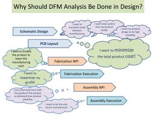
Design For Manufacturing (DFM) Making a Printed Circuit Board (PCB). by Prof. Bitar. Major Steps. Schematic Capture/ Simulation Tool. Net List. PCB Layout Tool. Gerber Files NC Drill File. Board Manufacturer. Schematic Capture / Simulation Example: Multisim. NET LIST REPORT.

E N D
Design For Manufacturing (DFM)Making a Printed Circuit Board (PCB) by Prof. Bitar
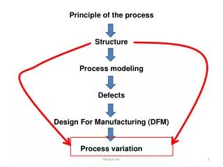
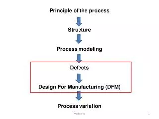
Major Steps Schematic Capture/ Simulation Tool Net List PCB Layout Tool Gerber Files NC Drill File Board Manufacturer
Schematic Capture / SimulationExample: Multisim NET LIST REPORT
Example Net List Netlist Report (From Document: Demo_BinaryClock_WPI) (Printed Date: April 14, 2009 00:21:13) ----------------------------------------------------------------------------- Net Page Component Pin ----------------------------------------------------------------------------- 1 Demo_BinaryClock SIP1 P2 _WPI 1 Demo_BinaryClock LED7 K _WPI 10 Demo_BinaryClock U5D 4Y _WPI 10 Demo_BinaryClock U6C 3A _WPI 11 Demo_BinaryClock LED7 A _WPI
Gerber Files / NC Drill File Silk Screen Copper Top Copper Bottom Solder Mask Top Solder Mask Bottom NC Drill File
NC Drill File M48 INCH,TZ VER,1 FMAT,2 DETECT,ON ATC,ON T1C0.12500 T2C0.02500 T3C0.04667 T4C0.03500 T5C0.03917 T6C0.04400 T7C0.04724 T8C0.03543 T9C0.05000 % T1 X0.20000Y0.20000 Y3.80000 X5.80000Y0.20000 Y3.80000 T2 X0.98000Y1.09000