Download
1 / 2
20 likes | 157 Views
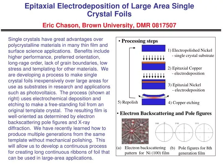
Processing steps. 1) Electropolished Nickel - single crystal substrate. 2) Epitaxial Copper - electrodeposition. 3) Epitaxial Nickel - electrodeposition. 5) Repolish. 4) Copper etching. Electron Backscattering and Pole figures.

E N D
Processing steps 1) Electropolished Nickel - single crystal substrate 2) Epitaxial Copper - electrodeposition 3) Epitaxial Nickel - electrodeposition 5) Repolish 4) Copper etching • Electron Backscattering and Pole figures • Electron backscattering pattern for Ni (100) film Epitaxial Electrodeposition of Large Area Single Crystal FoilsEric Chason, Brown University, DMR 0817507 Single crystals have great advantages over polycrystalline materials in many thin film and surface science applications. Benefits include higher performance, preferred orientation, long-rage order, lack of grain boundaries, low stress and templating for other materials. We are developing a process to make single crystal foils inexpensively over large areas for use as substrates in research and applications such as photovoltaics. The process (shown at right) uses electrochemical deposition and etching to make a free-standing foil from an original template crystal. The resulting film is well-oriented as determined by electron backscattering pole figures and X-ray diffraction. We have recently learned how to produce multiple generations from the same template without mechanical polishing. This will allow us to develop a continuous process for creating long continuous ribbons of foil that can be used in large-area applications. • Pole figures for 8th generation film
Cu 1 m Ni 1 m Sacrificial Layer Deposition Selective Single crystal Deposition Etching Inexpensive Single Crystal Substrates for Thin Film ApplicationsEric Chason, Brown University, DMR 0817507 Single crystal materials have better performance than polycrystalline materials in many thin film applications (e.g., superconductivity, photovoltaics, catalysts, opto- and micro-electronics, magnetic storage, etc.), but their use is often restricted by their high cost. We are developing a method to make large area single crystal foils to use as inexpensive substrates to expand the range of single crystal applications. The process we are developing (shown schematically at left) uses electrochemical methods to reproduce single crystals from a template layer. Much like a printing press, the template is reused to efficiently and inexpensively produce long ribbons with large surface area. We are working with collaborators to grow advanced materials (e.g., solar cells, graphene) on these substrates. 1 m • Steps for making single crystal foil 1) Single crystal substrate 2) Sacrificial layer deposition 3) Single crystal deposition 4) Selective etching • Process for making continuous ribbon