Download
1 / 13
170 likes | 510 Views
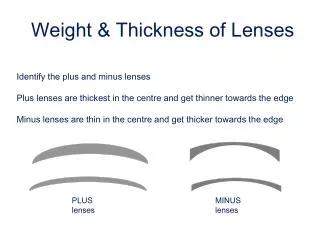
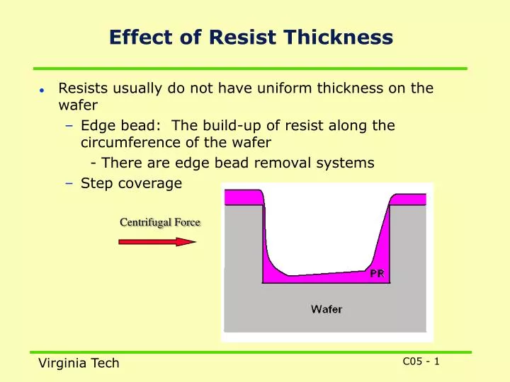
Effect of Resist Thickness. Resists usually do not have uniform thickness on the wafer Edge bead: The build-up of resist along the circumference of the wafer - There are edge bead removal systems Step coverage. Centrifugal Force. Effect of Resist Thickness.

E N D
Effect of Resist Thickness • Resists usually do not have uniform thickness on the wafer • Edge bead: The build-up of resist along the circumference of the wafer • - There are edge bead removal systems • Step coverage Centrifugal Force
Effect of Resist Thickness • The resist can be underexposed where it is thicker and overexposed where it is thinner • This can lead to linewidth variations • Light intensity varies with depth below the surface due to absorptionwhere is the optical absorption coefficient • Thus, the resist near the surface is exposed first • We have good fortune. There is a process called bleaching in which the exposed material becomes almost transparent • i.e., decreases after exposure to light • - Therefore, more light goes to deeper layers
aexposed = B and aunexposed = A+B C. A. Mack, “Absorption and exposure in positive photoresist”, Appl. Opt. 27(23), Dec. 1, 1988, pp. 4913-4919.
Photoresist Absorption • If the photoresist becomes transparent, and if the underlying surface is reflective, reflected light from the wafer will expose the photoresist in areas we do not want it to. • However, this leads to the possibility of standing waves (due to interference), with resultant waviness of the developed resist • We can solve this by putting an antireflective coating on the surface before spinning the photoresist increases process complexity
Standing Waves Due to Reflections http://www.lithoguru.com/scientist/lithobasics.html
Removal of Standing Wave Pattern (a) (b) (c) Diffusion during a post-exposure bake (PEB) is often used to reduce standing waves. Photoresist profile simulations as a function of the PEB diffusion length: (a) 20nm, (b) 40nm, and (c) 60nm. http://www.lithoguru.com/scientist/lithobasics.html
Mask Engineering • There are two ways to improve the quality of the image transferred to the photoresist • Optical Proximity Correction (OPC) • Phase Shift Masks (PSM) • We note that the lenses in projections systems are both finite and circular • Most features on the mask are square • We lose the high frequency components of the pattern • We thus lose information about the “squareness” of the corners
Mask Engineering • The effects are quite predictable • We can correct them by adjusting feature dimensions and shapes in the masks
Phase Shift Masks • In a projection system, the amplitudes of the diffracted light at the wafer add • Closely spaced lines interact; the intensity at the wafer is smeared • If we put a material of proper index of refraction on part of the mask, we can retard some of the light and change its phase by 180 degrees • Properly done, the amplitudes interfere • The thickness of the PS layer is n is the index of refraction of the phase shift material
Phase Shift Masks (PSM) Intensity pattern is barely sufficient to resolve the two patterns.