Download
1 / 13
270 likes | 808 Views
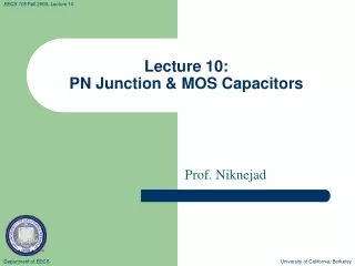
MOS Capacitors. ECE 2204. Some Classes of Field Effect Transistors. M etal- O xide- S emiconductor Field Effect Transistor MOSFET, which will be the type that we will study in this course. Me tal- S emiconductor Field Effect Transistor MESFET, typically fabricated with III-V semiconductors

E N D
MOS Capacitors ECE 2204
Some Classes of Field Effect Transistors • Metal-Oxide-Semiconductor Field Effect Transistor • MOSFET, which will be the type that we will study in this course. • Metal-Semiconductor Field Effect Transistor • MESFET, typically fabricated with III-V semiconductors • Junction Field Effect Transistor • JFET, resilient to electrostatic discharge (ESD) • High Electron Mobility Transistor or Modulation Doped Field Effect Transistor • HEMT or MODFET, typically fabricated with III-V semiconductors • Fast Reverse/Fast Recovery Epitaxial Diode • FREDFET • DNA Field Effect Transistor • The conduction path is through a strand of DNA
Field Effect Transistors • A voltage is applied to the gate of the transistor, which produces an electric field within the semiconductor. • Typically, the gate current is zero. • The conductivity (or resistivity) of the path between two contacts, the source and the drain, is altered by the voltage applied to the gate. • Device is also known as a voltage controlled resistor.
MOS Capacitor Oxide • The operation of a metal-oxide-semiconductor is used to explain the operation of the MOSFET. • In a MOSFET, the channel in the semiconductor, the oxide, and the gate metalization forms a MOS capacitor. • The structure looks like a parallel plate capacitor where one of the plates is the semiconductorand the other is the gate metalization. The insulator between the parallel plates is the oxide. Semiconductor
MOS Capacitor eOX =eoxeo where eoxis the relative dielectric constant of the oxide. eox tox
Operation of a MOS Capacitor • In the following analysis, it is assumed that the channel in the semiconductor is lightly doped with acceptors (i.e., p type). • There are three regions of operation • Accumulation (in this case, VG < 0 V) • Depletion (in this case, 0 V ≤ VG ≤ VTN) • Inversion (in this case, VG≥ VTN)
Accumulation (VG < 0 V) • An electric field E is induced by the applied voltage VG. • More holes are at the oxide-semiconductor interface than expected from the concentration of acceptors. • Holes are attracted to interface by the negative gate voltage. • Electrons are repelled towards the body contact.
Depletion (0 V < VG ≤ VTN) • The induced electric field E causes the concentration of holes at the oxide-semiconductor interface to be smaller than the acceptor concentration and the electron concentration to be greater than expected.
Depletion Mode Capacitance • The unscreened acceptors and a higher than expected electron concentration at the oxide semiconductor interface induce an electric field in the semiconductor, producing a depletion region to form.
Inversion (VG ≥ VTN) • The gate voltage is large enough that the concentration of electrons at the oxide-semiconductor interface is greater than the concentration of holes. • The type of the semiconductor has effectively been converted from p-type to n-type. The voltage when n = p at the oxide-semiconductor interface is called the threshold voltage, VTN.
Inversion Mode Capacitance • A depletion region still exists in the semiconductor, but is now located between the inverted (n-type) region and the remaining p-type semiconductor. • The thickness of the depletion region W is constant, even if VG increases so the magnitude of the MOS capacitance is constant.
MOS Capacitance • Is largest in the accumulation mode when VG ≤ 0 V • Is smallest in the inversion mode when VG≥ VTN • Varies with VGin the depletion mode
Questions • If the acceptor concentration is increased, will be threshold voltage have to increase or decrease? • Do you expect the threshold voltage to increase or decrease as the temperature of the MOS capacitor is increased? • Can you explain how the electron and hole concentration varies with VG if the semiconductor is initially n-type instead of p-type?