Download
1 / 14
140 likes | 214 Views
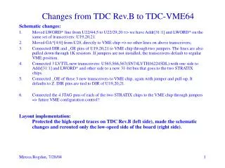
Introduction to TDC-II and Address Map. Mircea Bogdan (UC). TIME-TO-DIGITAL. TIME-TO-DIGITAL CONVERSION: 1.2ns sampling rate serdes_in ~ 20 ns LVDS pulse in the simulation window of QuartusII. TDC Board– Data Flow. TDC Chip – Data Flow. STRATIX-EP1S30F780C6- Block Diagram. Specifications.

E N D
Introduction to TDC-II and Address Map Mircea Bogdan (UC)
TIME-TO-DIGITAL TIME-TO-DIGITAL CONVERSION: 1.2ns sampling rate serdes_in ~ 20 ns LVDS pulse in the simulation window of QuartusII
TDC Chip – Data Flow STRATIX-EP1S30F780C6- Block Diagram
Specifications Edge detection: 1 hit = min 4 “1”bits followed by min 4 “0”bits; Records up to 7 hits/wire – max. number is VME controlled: 3 bits in Register 3; Choice of having the max. number of recorded hits/wire controlled for each L2A pulse with backplane pulses -> dynamic edge detector; The results are ready for VME read-out ~10 us after a L2A. Minimum time interval between successive L2A pulses: ~10 us. Front Panel ECL Calibration Pulse from the backplane or from the on-board Stratix Chip_0. The selection is made via VME. The local 12 ns pulse comes after each B0 with a VME controlled delay. Configuration of both Stratix chips can be restarted with one VME write operation. Configuration of the VME chip (all boards in crate) can be restarted from the backplane (P1/C12-SYSRESET*).
Name VME Address[31..0] Access Words Control reg. - Chip0 0xYY000000 : 0xYY00003C R/W CDF6998 Control reg. - Chip1 0xYY010000 : 0xYY01003C R/W CDF6998 Control reg. – VME Chip 0xYY020000 : 0xYY02003C R/W CDF6998 ID Prom – Chip0 0xYY100000 : 0xYY10003C R/O 16 ID Prom – Chip1 0xYY110000 : 0xYY11003C R/O 16 Hit_data_buffer – Chip0 0xYY800000 : 0xYY80017C R/W Max168 Hit_data_buffer – Chip1 0xYY810000 : 0xYY81017C R/W “ Hit_count_buffer – Chip0 0xYY900000 : 0xYY900014 R/W 7 Hit_count_buffer – Chip1 0xYY910000 : 0xYY910014 R/W 7 Test_data RAM – Chip0 0xYY700000 : 0xYY707FFC R/W 8192 Test_data RAM – Chip1 0xYY710000 : 0xYY717FFC R/W 8192 XFT_Out RAM – Chip0 0xYYA00000 : 0xYYA07FFC R/O 8192 XFT_Out RAM – Chip1 0xYYA10000 : 0xYYA17FFC R/O 8192 XFT_DAQ RAM – Chip0 0xYYB00000 : 0xYYB000FC R/O 128 XFT_DAQ RAM. – Chip1 0xYYB10000 : 0xYYB100FC R/O 128 Pulse Gen RAM – Chip0 (*) 0xYYC00000 : 0xYYC007FC R/W 512 Pulse Gen RAM – Chip1(*) 0xYYC10000 : 0xYYC107FC R/W 512 XFT_Setup RAM – Chip0 0xYYD00000 : 0xYYD0007C R/W 32 XFT_Setup RAM – Chip1 0xYYD10000 : 0xYYD1007C R/W 32 TDC Chips - General Address Map
Hit Count Word [31..0] - Format 31..28 27..24 23..20 19..16 15..12 11..8 7..4 3..0 Hit Count Channel 7 ……………………………………………. Hit Count Channel 1 Hit Count Channel 0 ……………………………………………………………………. Hit Count Channel 47 ……………………………………………. Hit Count Channel 41 Hit Count Channel 40 Readout Memory: Hit - Count Buffer Six actual Hit-Count VME words: each word has 8, 4-bit words, One 4-bit word for each wire: - Bit 3 is the channel ON/OFF status, - Bits 2..0 are the actual Hit Count Value. Header: 7..0 Bunch Crossing Counter; 17..8 number of hits in hit data block; 19..18 L2 Buffer number; 20 Unused: 0; 21 Chip serial number: 0 or 1; 22 TDC Type: 1; 31..23 Module ID – set with a VME write on Register 5.
Hit Data Word [31..0] - Format 31..24 23..16 15..8 7..0 Leading Edge[7..0] Width[7..0] Leading Edge[7..0] Width[7..0] Channel m, Hit1 0 < m < 47 Next Hit on same channel OR First hit on higher channel ……………………………………………………. Channel n, Hit j 0 < n < 47, 1 < j < 7 ……………………………………………………. Readout Memory: Hit - Data Buffer Each hit is recorded as a pair of Leading Edge[7..0], Pulse Width[7..0]. The number of newly recorded hits varies after each L2A pulse. The max number of Hit-Data words to read after a L2A pulse: - 16 bits/hit x 7 hits/channel x 48 channel/chip = 5376 bits/chip = 168 VME32 words/chip. Hit-Data VME readout buffer is never cleared -> it may include hits from old events.
XFT - Specs There are two modes of operation for the XFT Block • Old Style: • We are looking for four consecutive “1” bits (4.8 ns) in a window; • The same: PROMPT, NOTSURE and LATE windows from the old design; • Windows are set in units of 6ns; • The resulting P3 output data follow the same truth table as old TDC. • New Style (Specs are still in progress): • We are looking for four consecutive “1” bits (4.8 ns) in a window; • There are 11 time windows programmable in units of 6 ns that cover 396 ns; • The windows can be placed almost everywhere in the 396 ns time interval. • Maximum window coverage: ~ 260 ns; Have yet to determine if we use two different chip designs or if the “Old Stile” will be just a particular setup.
XFT DAQ • The XFT outputs are also routed to a buffer system, similar to the main one. • We have a Pipe-Line, 4 L2 Buffers and a VME read-out buffer, all with the same number of words as the main DAQ. • Differences: • buffer width (18 bits) and write clock (22ns); • this VME read-out buffer is not available for CBLT; • Pipe Size and L2 Buffer Length are adjustable independently from the main DAQ; • One can corroborate the Hit-Count/Data results with information from the XFT DAQ. • For testing, the chips have also a XFT-OUT-RAM, that has the XFT flags.
CBLT • The TDC Board permits CBLT transactions as per ANSI/VITA 23-1998. • Crate CPU starts block transfer from a “special” slot => a token passing mechanism => all modules are read successively in just one block transfer => readout time reduced. • From Slot 30, Addr YY900000 – Hit-Count Buffers – 14 words/board; • From Slot 31, Addr YY800000 – Hit-Data Buffers – max 192 words/board(4hits/wire). • Example for Hit-Count Buffers readout for 16 TDC boards in crate: • Regular VME: 32 read transfers @ 7 words each; • CBLT: 1 transfer @ 224 words. • In the test-crate at UC, measured approx. 200ns between successive _DTACK pulses, using MVME2301 with default timing settings.
CBLT Options • In CBLT transactions *BERR is asserted only by “Last” module, only at the end of transfer. • Readout options: • Crate CPU has special Error handler: • => interprets *BERR as end of transfer and deasserts *AS; • => don’t need to know how many words are there; • => can read Hit-Data before Hit-Count. • Crate CPU with no special Error handler (method tested in shop): • => have to know total number of words to read from crate; • => read Hit-Count words first (fixed number); • => calculate number of Hit-Data words; • => read Hit-Data buffers. • Yet to determine which method is better.
VME Chip Connects only to bits [15..0] of the VME Data Bus. Default state: CBLT enabled, Module not Last, Front Panel ECL pulses from backplane. After each event, the VME Chip has the number of new Hit-Data words in Register A. Using this info(one extra VME read), one can read Hit-Data Buffer before Hit-Count.