Download
1 / 11
110 likes | 267 Views
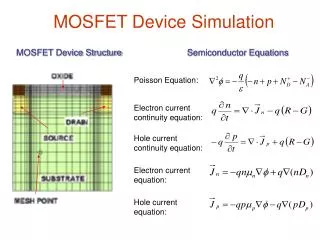
p*-n-n* diode CV characteristics changes at various contact and body doping concentrations. TCAD simulation Ernestas Zasinas, Rokas Bondzinskas, Juozas Vaitkus Vilnius University, Vilnius, Lithuania. Device doping profile and energy band structure. contact doping: p+ type,

E N D
p*-n-n* diode CV characteristics changes at various contact and body doping concentrations. TCAD simulation Ernestas Zasinas, Rokas Bondzinskas, Juozas Vaitkus Vilnius University, Vilnius, Lithuania
Device doping profile and energy band structure contact doping: p+ type, 1e17 – 1e20 cm-3 body doping: n-type 1e12 – 1e17 cm-3 contact doping: n+ type, 1e17 – 1e20 cm-3
This work is devoted to analyze the capacitance of p*nn* structure if the n region is differently compensated. • The role of doping in n* and p* regions is also analyzed. The TCAD Synopsys program was used for simulations. • The modeled device is a two dimensional p*nn* silicon based diode having p* contact region with gaussian doping profile of 2 m width and Np = 1019 cm-3 peak concentration. The n region homogeneous doping concentration Nd was variated within 1012 – 1017 cm-3. • The n* contact region doping profile was of gaussian type of variable 220 microns width and variable 1013 – 1020 cm-3 peak concentration N+. The device length L along direction perpendicular to junction planes was 50 and 300 m and its width W along the perpendicular dimension was chosen 600 m. • Sentaurus TCAD output results for the 2D device are presented as for the 3D device of 1 m height. The mesh along length direction was 1000-4000 points and only 3 points along width direction. Such a mesh efectively models one dimensional device.
Model equations (following Synopsys TCAD manual) Poisson Continuity equations Carrier transport (hydrodynamic model) Fermi statistics for band electrons and holes Shokley-Read-Hall recombination, doping dependent mobility were not specified. The CV characteristics were modeled at different donor doping concentrations and doping profiles of p*n and nn* junctions. Changing of donors concentrations in n and n* regions of the device effectively models its irradiation with a fluence of high energy particles of variable intensity, as long as the defects induced by these particles are mainly the types of acceptor traps which localize electrons thus reducing their concentration as a result of compensation.
Ldiode = 50 um Ldiode = 300 um CV characteristics for the diode with narrow (2 microns) n* contact region Characteristics are shown for several values of n base doping concentration (Nd) and n* peak concentration (N+). In some cases ((b) panel, blue and green curves) depletion is not reached at reasonable experimental values - depletion is possible only theoretically.
Ldiode = 50 um Ldiode = 300 um CV characteristics for the diode with wide (20 microns) n* contact region Characteristics are shown for several values of n base doping concentration (Nd) and n* peak concentration (N+). The ratio of concentrations is N+ /Nd = 10 When n* contact region is wide some 1/C2 -V curves have two kinks signaling about two separate inputs to depletion effect from two junctions p-n and n-n*
Ldiode = 50 um Ldiode = 300 um ( Similar to previous slide but N+ /Nd = 100 ) CV characteristics for the diode with wide (20 microns) n* contact region Characteristics are shown for several values of n base doping concentration (Nd) and n* peak concentration (N+). The ratio of concentrations is N+ /Nd = 100 When n* contact region is wide some 1/C2 -V curves have two kinks signaling about two separate inputs to depletion effect from two junctions p-n and n-n*
Ldiode = 300 um Ldiode = 50 um ( Similar to previous slide but N+ /Nd = 1000 ) CV characteristics for the diode with wide (20 microns) n* contact region Characteristics are shown for several values of n base doping concentration (Nd) and n* peak concentration (N+). The ratio of concentrations is N+ /Nd = 1000 When n* contact region is wide some 1/C2 -V curves have two kinks signaling about two separate inputs to depletion effect from two junctions p-n and n-n*
To explain the origin of the doubly kinked CV characteristic we suggest to present the p*nn* diode capacitance as a series of connected p*n and nn* capacitances. To see if this is correct we have recorded the dependence of potential Phi in the middle of p*nn* diode on the applied external voltage U. p-n-n* diode modeled by two sequential junctions: p-n and n-n* (device length 50 um n* contact length 20 um Nd = 1012cm-3, N+ = 1015cm-3) 2) during calculation of p-n-n* diiode C-V potential φ(V) dependence at the half of diode length is recorded 1) calculated C-V for two seperate p-n and n-n* junctions (each of half of the p-n-n* diode length)
Then we have simulated the CV characteristic of p*n junction and nn* junction devices having the same doping profile as they were in p*nn* diode junctions but their length being only half of the diode length. Having obtained functions C(U) for both junctions one may present the resulting capacitance of diode as: This formula was applied and the result (circles) was compared with p-n-n* diodes C-V (line) Apart from perfect coincidence Figure 6 also demonstrates that the sharp kink in the CV ( and 1/C2(V) ) occuring at U ~ 370 380 V originates itself from the nn* junction capacitance which saturates at ~170 180 V. Exactly the same voltage ( U – phi ) falls on the half of diode with nn* junction when the external voltage U = 370380 V is applied (see corresponding earlier figure).
Acknowledgements. This work was supported by the Lithuanian Academy of Sciences by project CERN-VU-2 Thank You for attention!