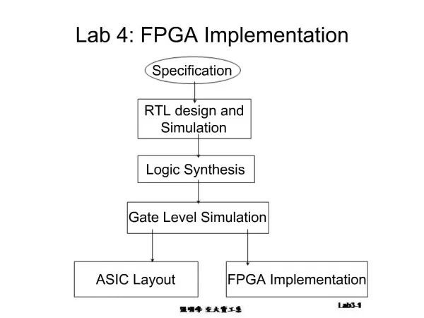
Download
1 / 29
320 likes | 338 Views
UNIT 2: Data Flow description. OBJECTIVES • Understand the concept of data flow description •Identify the basic statements and components of data flow •Review and understand the fundamentals of some digital logic systems such as half adder, 2x1 multiplexer, 2x2 combinational array

E N D
UNIT 2: Data Flow description OBJECTIVES •Understand the concept of data flow description •Identify the basic statements and components of data flow •Review and understand the fundamentals of some digital logic systems such as half adder, 2x1 multiplexer, 2x2 combinational array multiplier, 2-bit comparator, D-latch, ripple-carry adder, and carry-lookahead Adder. HDL Programming Fundamentals
2.1Highlights of Data Flow Description • Data flow description simulates the system by showing how the signal flows • from the input of the system to its output. The Boolean function of the • output or the logical structure of the system shows such signal flow. • Signal assignment statements are concurrent. At any simulation time, all signal • assignment statements that have an event are executed concurrently. HDL Programming Fundamentals
2.2 Structure of Data Flow Description Listing 2.1 Example of HDL Data Flow Description. entity system is port (I1, I2 : in bit; O1, O2 : out bit); end; architecture dtfl_ex of system is begin O1 <= I1 and I2; -- statement 1. O2 <= I1 xor I2; -- statement 2. --Statements 1 and 2 are signal assignment statements end dtfl_ex; HDL Programming Fundamentals
2.2.1 Signal Declaration and Assignment Statements signal s1, s2: bit; HDL Programming Fundamentals 2.2.2 Concurrent Signal Assignment Statement See slide 4 All statements that have event (s) on the right hand side are executed concurrently
event event event event I2 event event I1 event event O1 10 ns Calculate 0 and 1 =0 Assign 0 Calculate 0 and 1 =0 Assign 0 Calculate 1 and 1 =1 Assign 1 Calculate 1 and 1 =1 Assign 1 HDL Programming Fundamentals O1 <= I1 and I2 after 10 ns; O1 <= I1 and I2; Can you do the same for O2?
2.2.3Constant Declaration and Assignment Statements Constant period: time := 100 ns; HDL Programming Fundamentals
Example 2.1 Data Flow Description of a Half Adder Listing 2.2 HDL Programming Fundamentals
2.2.4 Assigning Delay Time to Signal Assignment Statement S1 <= sel and b after 10ns; ………(VHDL) assign #10 S1 = sel & b …………(Verilog). The 10 in Verilog code is 10 screen units HDL Programming Fundamentals
Example 2.2 2x1 Multiplexer with active low enable Input Output SEL Gbar Y X H L L L A H L B Y = (G and A and or (G and B and SEL); G is the invert of Gbar HDL Programming Fundamentals
library IEEE; use IEEE.STD_LOGIC_1164.ALL; entity mux2x1 is port (A,B,SEL, Gbar: in std_logic; Y: out std_logic); end mux2x1; architecture MUX_DF of mux2x1 is signal S1, S2, S3,S4, S5 : std_logic; Constant dly : time := 7 ns; -- replace all 7 ns with dly. Begin -- Assume 7 nano seconds propagationdelay -- for all and, or, and not. st1: Y <= S4 or S5 after 7 ns; st2: S4 <= A and S2 and S1 after 7 ns; st3: S5 <= B and S3 and S1 after 7 ns; st4: S2 <= not SEL after 7 ns; st5: S3 <= not S2 after 7 ns; st6: S1 <= not Gbar after 7 ns; end MUX_DF; HDL Programming Fundamentals
2.3 Data Type-Vectors signal a:bit_vector (3 downto 0)……….VHDL wire [3:0] a………….Verilog signal a:bit_vector (0 to 3)……….VHDL wire [0:3] a………….Verilog HDL Programming Fundamentals
Example 2.3 2x2 Unsigned combinational array multiplier HDL Programming Fundamentals
Example 2.3 2x2 Unsigned combinational array multiplier Downto versus to If P = 7, downto 0111 to 1110 library IEEE; use IEEE.STD_LOGIC_1164.ALL; entity mult_arry is port(a,b: in std_logic_vector(1 downto 0); P: out std_logic_vector (3 downto 0)); end mult_arry; architecture MULT_DF of mult_arry is begin --For simplicity propagation delay times are not considered -- in this example. P(0) <= a(0) and b(0); P(1) <= (a(0) and b(1)) xor (a(1) and b(0)); P(2) <= (a(1) and b(1)) xor ((a(0) and b(1)) and (a(1) and b(0))); P(3) <= (a(1) and b(1)) and ((a(0) and b(1))and (a(1) and b(0))); end MULT_DF; HDL Programming Fundamentals
Example 2.4 D-Latch InputsNext state E D Q current stateQ+ 0 x 0 0 0 x 1 1 1 0 x 0 1 1 x 1 _ _ Q = EQ + ED Qbar = Q HDL Programming Fundamentals Latch-level sensitive. When E=1, Q = D otherwise Q retains its previous value Flip-flop, edge sensitive. When edge of E, Q=D otherwise Q retains its previous value
HDL Programming Fundamentals _ _ Q = EQ + ED Qbar = Q
Example 2.4 D-latch library IEEE; use IEEE.STD_LOGIC_1164.ALL; entity D_Latch is port (D, E: in std_logic; Q, Qbar: buffer std_logic); -- Q and Qbar are declared as buffer because they act as both input and --output, they appearon the right and left hand side of signalassignment --statements. inout or linkage couldhave been used instead of buffer. end D_Latch; architecture DL_DtFl of D_Latch is constant Delay_EorD: Time:= 9 ns; constant Delay_inv : Time := 1 ns; begin --Assume 9 nsec propagation delay time between E or D and Qbar; and 1 nsec -- between Qbar and Q. Qbar <=(D and E) nor (not E and Q)after Delay_EorD; Q <= not Qbar after Delay_inv; end DL_DtFl; HDL Programming Fundamentals
HDL Programming Fundamentals _ _ Above waveform is for Q = EQ + ED , Qbar = Q Compare between latch and Flip-Flop. What would be the waveform for FF?
In Class Practice 2.2 Write a data-flow description (both VHDL and Verilog) of a system that has three 1-bit inputs a(1), a (2), and a (3), and one 1-bit output b. a(1) is the least significant bit. b is 1 only when {a(1)a(2)a(3)}= 1,3, 6 or 7 (all in decimal), otherwise 0. Derive a minimized Boolean function of the system and write the data flow description. Simulate the system and verify it is working as designed. What is the function of this system? Input Output a(3) a(2) a(1) b 0 0 0 0 0 0 1 1 0 1 0 0 0 1 1 1 1 0 0 0 1 0 1 0 1 1 0 1 1 1 1 1 HDL Programming Fundamentals a(1) 0 2X1 MUX b The system is 2x1 multiplexer a(2) 1 a(3)
--Program for prob 2.2 library IEEE; use IEEE.STD_LOGIC_1164.ALL; entity probl2_2 is port ( a : in std_logic_vector (3 downto 1); b: out std_logic); end probl2_2; architecture dataflow of probl2_2 is begin b <= ((not a(3)) and a(1)) or (a(3) and a(2)); end dataflow ; --bit could have been used instead of std_logic. --Since no delay time is specified we wrote one Boolean equation of the system; if --delay time is required, we have to use intermediate signals to describe the invert -- of a3, the “and”, and the “or” HDL Programming Fundamentals
Verilog 1.3.2 Structure of Verilog Module module half_adder (I1,I2, O1, O2); input I1; input I2; output O1; output O2; //Blank lines are allowed assign O1 = I1 ^ I2; //statement 1 assign O2 = I1 & I2; // statement 2 endmodule Verilog is case Sensitive A ≠ a ADDR ≠ ADDr HDL Programming Fundamentals 1.3.2.1 Verilog Ports input: the port is an input port only, the port is read. output: the port is an output port. The port, in contrast to VHDL output port, may appear in both sides of the assignment statement. inout: the port can be used as both input and output. The inout port is representing a bidirectional buss.
VHDL Commands or Components Verilog Counterpart entity module <= assign and, or, xor, not &, |, ^, ~ signal wire after # in, out, inout input, output, inout ( ) [ ] module mux2x1(A,B,SEL,Gbar,Y); input A,B,SEL,Gbar; output Y; wire S1,S2,S3,S4,S5; /* Assume 7 time units delay for all and, or, not. In Verilog we can not use specific time units such as nano seconds, the delay here is expressed in simulation screen units. */ assign #7 Y = S4 | S5; // st1. assign #7 S4 = A & S2 & S1; // st2 assign #7 S5 = B & S3 & S1; //st3 assign #7 S2 = ~ SEL; //st4 assign #7 S3 = ~ S2; //st5 assign #7 S1 = ~ Gbar; // st6 endmodule HDL Programming Fundamentals As in VHDL, all signal assignment statements (st1-st6) that have an event in the right hand side are executed concurrently. Execution is done, as in VHDL, in two phases: Calculate and Assign
b) Verilog 2x2 unsigned comb. Array multiplier (Listing 2.4) module mult_arry(a,b,P); input [1:0] a,b; output [3:0] P; /*For simplicity, propagation delay times are not considered in this example.*/ assign P[0] = a[0] & b[0]; assign P[1] = (a[0] & b[1]) ^ (a[1] & b[0]); assign P[2] = (a[1] & b[1]) ^ ((a[0] & b[1]) & (a[1] & b[0])); assign P[3] = (a[1] & b[1]) & ((a[0] & b[1])& (a[1] & b[0])); endmodule HDL Programming Fundamentals
In Class Practice 2.2 Write a data-flow description (both VHDL and Verilog) of a system that has three 1-bit inputs a(1), a (2), and a (3), and one 1-bit output b. a(1) is the least significant bit. b is 1 only when {a(1)a(2)a(3)}= 1,3, 6 or 7 (all in decimal), otherwise 0. Derive a minimized Boolean function of the system and write the data flow description. Simulate the system and verify it is working as designed. USE VERILOG module prob2_2(a,b); input [3:1]a; output b; assign b= (~a[3] & a[1]) | (a[3] & a[2]); endmodule HDL Programming Fundamentals
Example 2.5 2-bit Magnitude Comparator Listing 2.6 Both VHDL and Verilog HDL Programming Fundamentals
Case Study 2.1 Adders Listing 2.7 HDL Programming Fundamentals Ripple Carry Adder
HDL Programming Fundamentals Look-ahead Adder
2.4 Summary HDL Programming Fundamentals