Download
1 / 21
210 likes | 375 Views
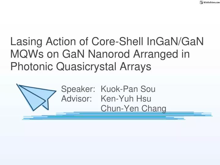
Lasing Action of Core-Shell InGaN / GaN MQWs on GaN Nanorod Arranged in Photonic Quasicrystal Arrays. Speaker: Kuok-Pan Sou Advisor: Ken- Yuh Hsu Chun-Yen Chang. Introduction Motivation Experiment Fabrication Result and Discussion Crystalline Measurement Optical Measurement

E N D
Lasing Action of Core-Shell InGaN/GaN MQWs on GaNNanorod Arranged in Photonic Quasicrystal Arrays Speaker: Kuok-Pan Sou Advisor: Ken-Yuh Hsu Chun-Yen Chang
Introduction • Motivation • Experiment • Fabrication • Result and Discussion • Crystalline Measurement • Optical Measurement • Conclusion Outline
Introduction • Motivation • Experiment • Fabrication • Result and Discussion • Crystalline Measurement • Optical Measurement • Conclusion Outline
Introduction GaN-base Laser
Introduction • Motivation • Experiment • Fabrication • Crystalline Measurement • Optical Measurement • Result and Discussion • Conclusion Outline
Low Dimensional Structure Motivation Quantum Dot Quantum Wire Quantum Well Super Lattice PIC PIC PIC Enhance Efficiency Low Threshold Quantum Confine Effect
How to fabricated GaN array Motivation Bottom up Top down
Introduction • Motivation • Experiment • Fabrication….. • Result and Discussion • Crystalline Measurement • Optical Measurement • Conclusion Outline
Dry Etching GaN Regrowth Nanoimprint Lithography Bulk c-GaN Fabrication MQW: InGaN/GaN × 6 pairs
Introduction • Motivation • Experiment • Fabrication….. • Result and Discussion • Crystalline Measurement • Optical Measurement • Conclusion Outline
Defect Reduction • Defect reduced by Nano-imprint lithography
12-fold symmetryphotonic quasi-crystal Defect Reduction & The Enlarged MQWs (Gain Material) • Dislocation density: One order↓ • The enlarged active area by the factor of 5
Introduction • Motivation • Experiment • Fabrication….. • Result and Discussion • Crystalline Measurement • Optical Measurement • Conclusion Outline
uPL Measurement Q~1155 Radius~27um Spotsize~ 2290um^2
(a) (c) 369 nm (b) CL Mapping (e) 440 nm (d) 420 nm (f) 460 nm 500 480 460 440 420 (h) 500 nm (i) 520 nm (g) 480 nm • Red shift from bottom to middle portion of nanorods • Gradient Indium content distribution
Characteristic Temperature Ith(T)=I0 Exp(T/T0) GaNVCSELT0=180~220K
Introduction • Motivation • Experiment • Fabrication • Result and Discussion • Crystalline Measurement • Optical Measurement • Conclusion Outline
Good Job • Thank YOU !! Kidding Day
No Kidding • Be Fun !! Q&A