Download
1 / 20
200 likes | 333 Views
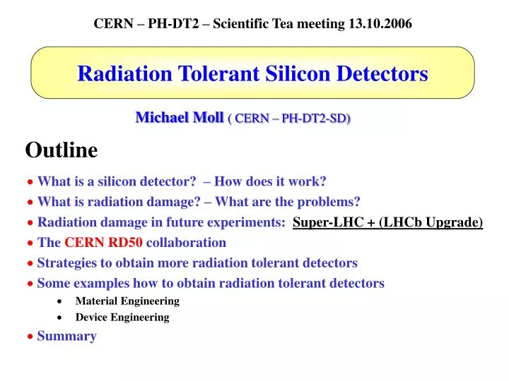
CERN – PH-DT2 – Scientific Tea meeting 13.10.2006. Radiation Tolerant Silicon Detectors. Outline. What is a silicon detector? – How does it work? What is radiation damage? – What are the problems? Radiation damage in future experiments: Super-LHC + (LHCb Upgrade)

E N D
CERN – PH-DT2 – Scientific Tea meeting 13.10.2006 Radiation Tolerant Silicon Detectors Outline • What is a silicon detector? – How does it work? • What is radiation damage? – What are the problems? • Radiation damage in future experiments: Super-LHC + (LHCb Upgrade) • The CERN RD50 collaboration • Strategies to obtain more radiation tolerant detectors • Some examples how to obtain radiation tolerant detectors • Material Engineering • Device Engineering • Summary Michael Moll ( CERN – PH-DT2-SD)
Silicon Detector – Working principle • Take a piece of high resistivity silicon and produce two electrodes (not so easy !) • Apply a voltage in order to create an internal electric field (some hundred volts over the 0.3mm thick device) • Traversing charged particles will produce electron-hole pairs • The moving electrons and holes will create a signal in the electric cicuit Michael Moll – PH-DT2 – Scientific Tea, 11 October 2006 -2 / 20-
pitch Silicon Strip Detector • Segmentation of the p+ layer into strips (Diode Strip Detector) and connection of strips to individual read-out channels gives spatial information typical thickness: 300mm (150m - 500m used) • using n-type silicon with a resistivity of = 2 KWcm (ND ~2.2.1012cm-3) results in a depletion voltage ~ 150 V • Resolution depends on the pitch p (distance from strip to strip) • - e.g. detection of charge in binary way (threshold discrimination) and using center of strip as measured coordinate results in: • typical pitch values are 20 mm– 150 mm 50 mm pitch results in 14.4 mm resolution Michael Moll – PH-DT2 – Scientific Tea, 11 October 2006 -3 / 20-
Example – The ATLAS module Michael Moll – PH-DT2 – Scientific Tea, 11 October 2006 -4 / 20-
LHCb – VELO: Silicon sensor details R-measuring sensor (45 degree circular segments) • 300 mm thick sensors • n-on-n, DOFZ wafers • 42 mm radius • AC coupled, double metal • 2048 strips / sensor • Pitch from 40 to 100 mm • Produced by Micron Semiconductor 42 mm 8 mm F-measuring sensor (radial strips with a stereo angle) [Martin van Beuzekom, STD6, September 2006] Michael Moll – PH-DT2 – Scientific Tea, 11 October 2006 -5 / 20-
LHCb-VELO - Module construction Beetle • 4 layer kapton circuit • Heat transport with TPG • Readout with 16 Beetle chips • 128 channels, 25 ns shaping time, • analog pipeline • 0.25 mm CMOS • no performance loss up to 40 Mrad • Yield > 80 % Kapton hybrid Carbon fibre Thermal Pyrolytic Graphite (TPG) [Martin van Beuzekom, STD6, September 2006] Michael Moll – PH-DT2 – Scientific Tea, 11 October 2006 -6 / 20-
Motivation for R&D on Radiation Tolerant Detectors: Super - LHC 5 years 10 years 2500 fb-1 500 fb-1 • LHC upgradeLHC (2007), L = 1034cm-2s-1f(r=4cm) ~3·1015cm-2 • Super-LHC (2015 ?), L = 1035cm-2s-1f(r=4cm) ~1.6·1016cm-2 • LHC (Replacement of components)e.g. - LHCb Velo detectors (~2010) - ATLAS Pixel B-layer (~2012) • Linear collider experiments (generic R&D)Deep understanding of radiation damage will be fruitful for linear collider experiments where high doses of e, g will play a significant role. 5 Michael Moll – PH-DT2 – Scientific Tea, 11 October 2006 -7 / 20-
Overview: Radiation Damage in Silicon Sensors • Two general types of radiation damage to the detector materials: Bulk (Crystal) damagedue to Non Ionizing Energy Loss (NIEL) - displacement damage, built up of crystal defects – • Change of effective doping concentration(higher depletion voltage, under- depletion) • Increase of leakage current (increase of shot noise, thermal runaway) • Increase of charge carrier trapping(loss of charge) Surface damagedue to Ionizing Energy Loss (IEL) - accumulation of positive in the oxide (SiO2) and the Si/SiO2 interface –affects: interstrip capacitance (noise factor), breakdown behavior, … • Impact on detector performance and Charge Collection Efficiency (depending on detector type and geometry and readout electronics!)Signal/noise ratio is the quantity to watch Sensors can fail from radiation damage ! Michael Moll – PH-DT2 – Scientific Tea, 11 October 2006 -8 / 20-
The charge signal Most probable charge ≈ 0.7 mean Mean charge noise Cut (threshold) • Collected Charge for a Minimum Ionizing Particle (MIP) • Mean energy loss dE/dx (Si) = 3.88 MeV/cm 116 keV for 300m thickness • Most probable energy loss≈ 0.7 mean 81 keV • 3.6 eV to create an e-h pair 72 e-h / m (mean) 108 e-h / m (most probable) • Most probable charge (300 m)≈ 22500 e ≈ 3.6 fC Michael Moll – PH-DT2 – Scientific Tea, 11 October 2006 -9 / 20-
Signal to Noise ratio What is signal and what is noise? more noise less signal • Landau distribution has a low energy tail - becomes even lower by noise broadening • Noise sources: (ENC = Equivalent Noise Charge) - Capacitance - Leakage Current - Thermal Noise (bias resistor) • Good hits selected by requiring NADC > noise tail If cut too high efficiency loss If cut too low noise occupancy • Figure of Merit: Signal-to-Noise Ratio S/N • Typical values >10-15, people get nervous below 10. Radiation damage severely degrades the S/N. Michael Moll – PH-DT2 – Scientific Tea, 11 October 2006 -10 / 20-
The CERN RD50 Collaborationhttp://www.cern.ch/rd50 RD50: Development of Radiation Hard Semiconductor Devices for High Luminosity Colliders • Collaboration formed in November 2001 • Experiment approved as RD50 by CERN in June 2002 • Main objective: Development of ultra-radiation hard semiconductor detectors for the luminosity upgrade of the LHC to 1035 cm-2s-1 (“Super-LHC”). Challenges: - Radiation hardness up to 1016 cm-2 required - Fast signal collection (Going from 25ns to 10 ns bunch crossing ?) - Low mass (reducing multiple scattering close to interaction point) - Cost effectiveness (big surfaces have to be covered with detectors!) • Presently 261 members from 52 institutes Belarus (Minsk), Belgium (Louvain), Canada (Montreal), Czech Republic (Prague (3x)), Finland (Helsinki, Lappeenranta), Germany (Berlin, Dortmund, Erfurt, Freiburg, Hamburg, Karlsruhe), Israel (Tel Aviv), Italy (Bari, Bologna, Florence, Padova, Perugia, Pisa, Trento, Turin), Lithuania (Vilnius), The Netherlands (Amsterdam),Norway (Oslo (2x)), Poland (Warsaw (2x)), Romania (Bucharest (2x)),Russia (Moscow), St.Petersburg), Slovenia (Ljubljana), Spain (Barcelona, Valencia), Switzerland (CERN, PSI), Ukraine (Kiev), United Kingdom(Exeter, Glasgow, Lancaster, Liverpool, Sheffield, University of Surrey), USA (Fermilab, Purdue University, Rochester University, SCIPP Santa Cruz, Syracuse University, BNL, University of New Mexico) Michael Moll – PH-DT2 – Scientific Tea, 11 October 2006 -11 / 20-
Approaches to develop radiation harder solid state tracking detectors • Defect Engineering of SiliconDeliberate incorporation of impurities or defects into the silicon bulk to improve radiation tolerance of detectors • Needs: Profound understanding of radiation damage • microscopic defects, macroscopic parameters • dependence on particle type and energy • defect formation kinetics and annealing • Examples: • Oxygen rich Silicon (DOFZ, Cz, MCZ, EPI) • Oxygen dimer & hydrogen enriched Si • Pre-irradiated Si • Influence of processing technology • New Materials • Silicon Carbide (SiC), Gallium Nitride (GaN) • Diamond (CERN RD42 Collaboration) • Amorphous silicon • Device Engineering (New Detector Designs) • p-type silicon detectors (n-in-p) • thin detectors, epitaxial detectors • 3D detectors and Semi 3D detectors, Stripixels • Cost effective detectors • Monolithic devices Scientific strategies: • Material engineering • Device engineering • Change of detectoroperational conditions CERN-RD39“Cryogenic Tracking Detectors”operation at 100-200K to reduce charge loss Michael Moll – PH-DT2 – Scientific Tea, 11 October 2006 -12 / 20-
Silicon Materials under Investigation by RD50 • DOFZ silicon • Enriched with oxygen on wafer level, inhomogeneous distribution of oxygen • CZ silicon • high Oi (oxygen) and O2i (oxygen dimer) concentration (homogeneous) • formation of shallow Thermal Donors possible • Epi silicon • high Oi , O2i content due to out-diffusion from the CZ substrate (inhomogeneous) • thin layers: high doping possible (low starting resistivity) Michael Moll – PH-DT2 – Scientific Tea, 11 October 2006 -13 / 20-
Standard FZ, DOFZ, Cz and MCz Silicon 24 GeV/c proton irradiation • Standard FZ silicon • type inversion at ~ 21013 p/cm2 • strong Neff increase at high fluence • Oxygenated FZ (DOFZ) • type inversion at ~ 21013 p/cm2 • reduced Neff increase at high fluence • CZ siliconand MCZ silicon • no type inversion in the overall fluence range (verified by TCT measurements) (verified for CZ silicon by TCT measurements, preliminary result for MCZ silicon) donor generation overcompensates acceptor generation in high fluence range • Common to all materials (after hadron irradiation): • reverse current increase • increase of trapping (electrons and holes) within ~ 20% Michael Moll – PH-DT2 – Scientific Tea, 11 October 2006 -14 / 20-
EPI Devices – Irradiation experiments G.Lindström et al.,10th European Symposium on Semiconductor Detectors, 12-16 June 2005G.Kramberger et al., Hamburg RD50 Workshop, August 2006 • Epitaxial silicon • Layer thickness: 25, 50, 75 m (resistivity: ~ 50 cm); 150 m (resistivity: ~ 400 cm) • Oxygen: [O] 91016cm-3; Oxygen dimers (detected via IO2-defect formation) 105V (25mm) 230V (50mm) 320V (75mm) • Only little change in depletion voltage • No type inversion up to ~ 1016 p/cm2 and ~ 1016 n/cm2high electric field will stay at front electrode!reverse annealing will decreases depletion voltage! • Explanation: introduction of shallow donors is bigger than generation of deep acceptors • CCE (Sr90 source, 25ns shaping): 6400 e (150 mm; 2x10¹⁵ n/cm-2) 3300 e (75mm; 8x10¹⁵ n/cm-2) 2300 e (50mm; 8x10¹⁵ n/cm-2) Michael Moll – PH-DT2 – Scientific Tea, 11 October 2006 -15 / 20-
Device engineeringp-in-n versus n-in-p detectors p-type silicon after high fluences: n-type silicon after high fluences: n+on-p p+on-n • n-on-p silicon, under-depleted: • Limited loss in CCE • Less degradation with under-depletion • Collect electrons (fast) • p-on-n silicon, under-depleted: • Charge spread – degraded resolution • Charge loss – reduced CCE Be careful, this is a very schematic explanation,reality is more complex ! Michael Moll – PH-DT2 – Scientific Tea, 11 October 2006 -16 / 20-
no reverse annealing visible in the CCE measurement ! e.g. for 7.5 1015 p/cm2 increase of Vdep from Vdep~ 2800V to Vdep > 12000V is expected ! n-in-p microstrip detectors n-in-p: - no type inversion, high electric field stays on structured side - collection of electrons • n-in-p microstrip detectors (280mm) on p-type FZ silicon • Detectors read-out with 40MHz CCE ~ 6500 e (30%) after 7.5 1015 p cm-2 at 900V Michael Moll – PH-DT2 – Scientific Tea, 11 October 2006 -17 / 20-
n-columns p-columns wafer surface ionizing particle carriers collected at the same time n-type substrate 3D detector - concepts Introduced by: S.I. Parker et al., NIMA 395 (1997) 328 • “3D” electrodes: - narrow columns along detector thickness, - diameter: 10mm, distance: 50 - 100mm • Lateral depletion: - lower depletion voltage needed - thicker detectors possible - fast signal - radiation hard Michael Moll – PH-DT2 – Scientific Tea, 11 October 2006 -18 / 20-
3D detector - concepts Introduced by: S.I. Parker et al., NIMA 395 (1997) 328 • “3D” electrodes: - narrow columns along detector thickness, - diameter: 10mm, distance: 50 - 100mm • Lateral depletion: - lower depletion voltage needed - thicker detectors possible - fast signal - radiation hard n-columns p-columns wafer surface n-type substrate • Simplified 3D architecture • n+ columns in p-type substrate, p+ backplane • operation similar to standard 3D detector • Simplified process • hole etching and doping only done once • no wafer bonding technology needed • Simulations performed • Fabrication: • IRST(Italy), CNM Barcelona metal strip hole [C. Piemonte et al., NIM A541 (2005) 441] hole Hole depth 120-150mm Hole diameter ~10mm C.Piemonte et al., STD06, September 2006 • First CCE tests under way Michael Moll – PH-DT2 – Scientific Tea, 11 October 2006 -19 / 20-
Conclusion • New Materials like SiC and GaN have been characterized (not shown in this talk) . CCE tests show that these materials are not radiation harder than silicon Silicon (operated at e.g. -30°C) seems presently to be the best choice • At fluences up to 1015cm-2(Outer layers of SLHC detector) the depletion voltage change and the large area to be covered is major problem: • MCZ silicon detectors could be a cost-effective radiation hard solution • p-type (FZ and MCZ) silicon microstrip detectors show good results:CCE 6500 e; Feq=41015 cm-2, 300mm, collection of electrons, no reverse annealing observed in CCE measurement! • At the fluence of 1016cm-2(Innermost layer of a SLHC detector) the active thickness of any silicon material is significantly reduced due to trapping. New options: • Thin/EPI detectors : drawback: radiation hard electronics for low signals needede.g. 3300e at Feq 8x1015cm-2, 75mm EPI, …. thicker layers (150 mm presently under test) • 3D detectors : drawback: very difficult technology ….. steady progress within RD50 Further information: http://cern.ch/rd50/ Michael Moll – PH-DT2 – Scientific Tea, 11 October 2006 -20 / 20-