Download
1 / 30
300 likes | 467 Views
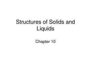
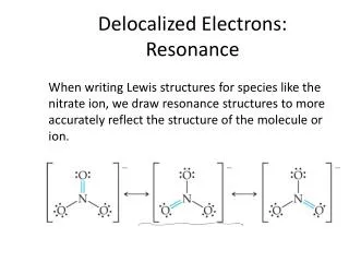
Do it with electrons !. Grey cast iron ( 灰色生 铁 ) - rather brittle. Ductile iron - highly ductile. Microscopy. Structure determines properties. We have discussed crystal structure (x-ray diffraction) But consider now different level of structure.

E N D
Grey cast iron (灰色生铁) - rather brittle Ductile iron - highly ductile Microscopy Structure determines properties We have discussed crystal structure (x-ray diffraction) But consider now different level of structure Microstructure (微观结构)- also affects properties
Microscopy Structure determines properties We have discussed crystal structure (x-ray diffraction) But consider now different level of structure Microstructure - also affects properties Cemented WC (碳化钨) cutting tool
Microscopy Structure determines properties We have discussed crystal structure (x-ray diffraction) But consider now different level of structure Microstructure - also affects properties Ferroelectric domains in BaTiO3
Microscopy Structure determines properties We have discussed crystal structure (x-ray diffraction) But consider now different level of structure Microstructure - also can be 'art (美术)'
Electron microscopy SEM - scanning electron microscopy tiny electron beam scanned across surface of specimen backscattered (背散射) or secondary electrons (二次电子) detected signal output to synchronized display
Electron microscopy SEM - scanning electron microscopy Magnification range 15x to 200,000x Resolution of 50 Å Excellent depth of focus Relatively easy sample prep
SEM - scanning electron microscopy Electron gun Don't make x-rays - use electrons directly Wavelength: NOT = hc/E (massless photons) = h/(2melectronqVo) (non-relativistic) = h/(2melectronqVo + q2Vo2/c2)1/2 (relativistic (相对论的))
SEM - scanning electron microscopy = h / (2melectronqVo + q2Vo2/c2)1/2 = 1.22639 / (Vo + 0.97845 · 10-6Vo2)1/2 (nm) & Vo(volts) 10 kV ——> 0.12 Å 100 kV ——> 0.037 Å
Electron emitter SEM - scanning electron microscopy Electron gun
SEM - scanning electron microscopy = h/(2melectronqVo + q2Vo2/c2)) Effects of increasing voltage in electron gun: Resolution increased ( decreased) Penetration increases Specimen charging increases (insulators) Specimen damage increases Image contrast decreases
SEM - scanning electron microscopy Field emission electron source: High electric field at very sharp tip causes electrons to "tunnel" maybe
SEM - scanning electron microscopy Field emission electron source: High electric field at very sharp tip causes electrons to "tunnel"
SEM - scanning electron microscopy Field emission electron source: High electric field at very sharp tip causes electrons to "tunnel" cool tip ——> smaller E in beam improved coherence many electrons from small tip ——> finer probe size, higher current densities (100X >) problems - high vacuum, more $$$, fussy
SEM - scanning electron microscopy Lenses electrons focused by Lorentz force from electromagnetic field F = qv x B effectively same as optical lenses Lenses are ring-shaped coils generate magnetic field electrons pass thru hollow center lens focal length is continuously variable apertures control, limit beam
SEM - scanning electron microscopy Specimen Conducting - little or no preparation attach to mounting stub for insertion into instrument may need to provide conductive path with Ag paint Non-conducting - usually coat with conductive very thin layer (Au, C, Cr)
SEM - scanning electron microscopy Specimen Can examine fracture surfaces electronic devices fibers coatings particles etc.
SEM - scanning electron microscopy Specimen Can be tilted, translated Specimen size limited by size of sample chamber
high energy compositional contrast low energy topographic contrast composition - EDS SEM - scanning electron microscopy Specimen What comes from specimen? Backscattered electrons Secondary electrons Fluorescent X-rays Brightness of regions in image increases as atomic number increases (less penetration gives more backscattered electrons)
SEM - scanning electron microscopy Backscattered electron detector - solid state detector electron energy up to 30-50 keV annular around incident beam repel secondary electrons with — biased mesh images are more sensitive to chemical composition (electron yield depends on atomic number) line of sight necessary
+ bias mesh needed in front of detector to attract low energy electrons line of sight unnecessary SEM - scanning electron microscopy Secondary electron detector - scintillation detector
SEM - scanning electron microscopy Choose correct detector- topography example Fracture surface in iron backscattered electrons secondary electrons
SEM - scanning electron microscopy Composition - what elements present at a particular spot in specimen? Use solid state detector Do energy scan for fluorescent X-rays
image X-ray map SEM - scanning electron microscopy Composition mapping - x-ray fluorescence Use solid state detector set for X-ray energy for a particular element in specimen
SEM - scanning electron microscopy Interaction volume Backscattered electrons come from whole volume (high energy) Secondary electrons come from neck only (low energy)
SEM - scanning electron microscopy Contrast Comes from any kind of interaction with electron beam topography composition elements phases grain (crystal) orientation charging affects contrast
SEM - scanning electron microscopy Magnification
SEM - scanning electron microscopy Resolution Determined by probe size
SEM - scanning electron microscopy Resolution Determined by probe size