Download

1 / 26
320 likes | 726 Views
National Instruments Multisim. What is Multisim? Multisim is a schematic capture and simulation application It consists of tools that assist you in carrying out the major steps in circuit design

E N D
National Instruments Multisim • What is Multisim? • Multisim is a schematic capture and simulation application • It consists of tools that assist you in carrying out the major steps in circuit design • Multisim is designed for schematic entry, simulation, and feeding to downstage steps, such as PCB layout.
Getting Started • Start > All Programs > Circuit Design Suite 11.0 • Multisim 11.0 • Ultiboard 11.0 • Documentation
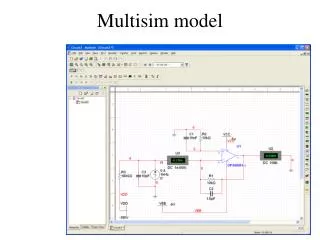
Multisim User Interface 1 Menu Bar 2 Design Toolbox 3 Component Toolbar 4 Standard Toolbar 5 View Toolbar 6 Simulation Toolbar 7 Main Toolbar 8 In Use List 9 Instruments Toolbar 10 Scroll Left/Right 11 Circuit Window 12 Spreadsheet View 13 Active Tab
Opening and Saving a File • When opening Multisim a blank file opens on the workspace called Design1 • Complete the following steps to save the file with a new name: • 1. Select File»Save As to display a standard Windows Save dialog. • 2. Navigate to the location where you wish the file to reside • 3. Select a filename, and click the Save button.
Placing Components • Select Place»Component to display the Select a Component dialog box • Select desired component and click OK, the component appears as a “ghost” on the cursor • Move the cursor to the workspace and left-click to place the component; notice the Reference Designator (ex: U1, R1)
Placing Components • When placing RLC components, type the value of the device that you want to place in the field at the top of the Component list • Crtl-R will change the orientation of the selected component • When a component is on the workspace and you want to place the same component again, highlight it and select Edit»Copy, then Edit»Paste. • You can also select it from the In Use List and click to place it on the workspace • When placing a AC or DC voltage source: double-click on it to change the Voltage (Pk) to desired amount then click OK
Wiring the Circuit • All components have pins that you use to wire them to other components or instruments • As soon as your cursor is over a pin, Multisim knows you want to wire and the pointer changes to a crosshair • Complete the following steps to wire the circuit: • 1. Click on a pin on a component to start the connection and move the mouse; a wire appears, attached to your cursor • 2. Click on a pin on the second component to finish the connection; Multisim automatically places the wire, which snaps to an appropriate configuration • Once you have wired a circuit, you can drop two-pinned components like resistors directly onto a wire; the connection is automatically made by Multisim
Simulations with Virtual Instruments • Select Simulate»Instruments»Oscilloscope to place an oscilloscope on the workspace and wire appropriately into circuit • Double-click on the scope’s icon to show the instrument face • Select Simulate»Run; the output of the opamp appears on the scope
Use AC Analysis to verify the frequency response of an amplifier Complete the following steps to perform an AC Analysis at the output of an opamp: 1. Double-click on the wire that is attached to output pin of the opamp, and change the net name to analog_out in the Net dialog box 2. Select Simulate» Analyses»AC Analysis and click on the Output tab 3. Highlight V(analog_out) in the left column and click Add; V(analog_out) moves to the right column; this will display the voltage at node V(analog_out) Analysis
Analysis with Grapher • Click Simulate; the results of the analysis appear in the Grapher The Grapher is a multi-purpose display tool that lets you view, adjust, save and export graphs and charts
Reports • You can generate a number of reports in Multisim: Bill of Materials (BOM), Component Detail Report, Netlist Report, Schematic Statistics, Spare Gates and the Cross Reference Report
Bill of Materials • A bill of materials lists the components used in your design and provides a summary of the components needed to manufacture the circuit board • Information provided includes: • Quantity of each component needed • Description, including the type of component (example: resistor) and value (example: 5.1 kohm) • Reference Designator of each component • Package or footprint of each component
Select Reports»Bill of Materials Can either Print or Save the BOM Bill of Materials intended to assist manufacturing, It includes only “real” components It excludes components that are not real or available for purchase, such as sources or virtual components Generating BOM
Ultiboard • Ultiboard is the PCB layout application of National Instruments Circuit Design Suite • Used to lay out and route printed circuit boards, perform certain basic mechanical CAD operations, and prepare them for manufacturing • Provides automated parts placement and layout
Ultiboard User Interface 1 Menu Bar 2 Standard Toolbar 3 Select Toolbar 4 Draw Settings Toolbar 5 View Toolbar 6 Main Toolbar 7 Autoroute Toolbar 8 Status Bar 9 Workspace 10 Spreadsheet View 11 Design Toolbox 12 3D Preview 13 Birds Eye View
Opening Multisim Design • Select File»Open Samples and double-click on your design
Creating Board Outline • There is already a board outline, however, you can create one that is a more suitable size for the parts in this design by: • Drawing tools • Import DXF file • Use Board Wizard
1. Double-click on Board Outline in the Layers tab to make it the active layer 2. Click on the existing board outline in the design and press <Delete> on the keyboard 3. Choose Tools»Board Wizard 4. Enable the Change the layer technology option to make the other options available 5. Choose Multi-layers constructed with double-sided boards and single layer stack-ups, and click Next Board Wizard
Board Wizard • In the Board Wizard - Shape of Board dialog box: • Make sure the Reference Point is set to Bottom-left for Alignment • Select Rectangular option • Set the Width and Height to desired dimensions • Set the Clearance to desired distance • This is the distance from the edge of the board that is to be kept free of any other elements. • Click Finish • The board outline is placed on your design
Placing Parts • Before you begin, double-click the Copper Top layer in the Design Toolbox to make it the active layer • Can place parts by: • Dragging them into place • Use the Parts tab in the Spreadsheet View to locate parts and place them • Select parts from the database
Placing Traces • You have the following options for placing traces: • Manual trace • Follow-me trace • Connection machine trace • A manual trace is placed exactly as you specify, even running through a component or trace if that is the path you set out • A follow-me trace automatically draws a legal trace between the pins you select with your mouse movements—you can move from pin to pin, leaving a legal trace • A connection machine trace automatically joins two pins by the most efficient route, though you have the option of changing it
Autoroute • Select Autoroute»Start Autoplacement • The parts are automatically placed on the circuit board • Select Autoroute»Start/Resume Autorouter. • The workspace switches to Autorouter Mode and trace autorouting begins • As autorouting proceeds, you will see traces being placed on the board • When autorouting is complete, Autorouter Mode closes and you are returned to the workspace • The autorouter can be stopped at any time and you can make manual changes as desired • When you restart the autorouter, it will continue with the changes you made
Cleaning up the Board • Before sending the board for manufacturing, you should clean up any open trace ends (trace segments that do not have any terminating connections in the design) and unused vias that have been left on the board • To delete open trace ends, click Edit»Copper Delete»Open Trace Ends • To delete any unused vias, make sure the design is open and click Design»Remove Unused Vias
Exporting Files • An exported file contains complete information describing how a finished board is to be manufactured • Files that can be exported include: • Gerber • RS-274X • RS-274D files