Download
1 / 45
480 likes | 671 Views
Carrier and Phonon Dynamics in InN and its Nanostructures. Yu-Ming Chang ( 張玉明 ) Center for Condensed Matter Sciences National Taiwan University April 12, 2007 Institute of Physics, NCTU. Outline. Motivation Time-resolved second-harmonic generation (TRSHG)

E N D
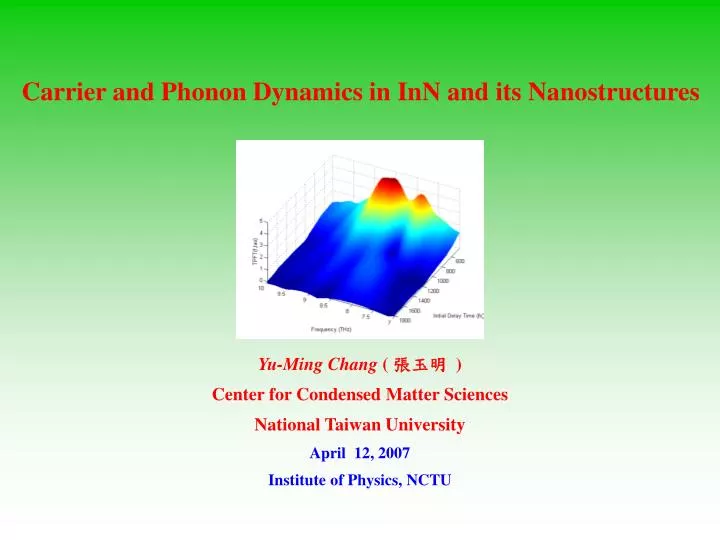
Carrier and Phonon Dynamics in InN and its Nanostructures Yu-Ming Chang ( 張玉明) Center for Condensed Matter Sciences National Taiwan University April 12, 2007 Institute of Physics, NCTU
Outline • Motivation • Time-resolved second-harmonic generation (TRSHG) • What is coherent phonon spectroscopy • Coherent phonon spectroscopy of InN and its nanostructures • Identification of surface optical phonon • Direct observation of LO phonon and plasmon coupling • Determination of the InN effective mass along the c-axis • Determination of the InN plasma relaxation time • Coherent phonon spectroscopy of InN ultrathin films • Conclusion
Question: What can we play in this ball game ? Our research strategy : Try to explore the transient carrier and phonon dynamics in InN and its nanostructures !
Femtosecond laser pump and probe technique D l t = 2Dl/c t BS To Sample Probe Pump Femtosecond Laser pulse Mirror
Time-resolved second-harmonic generation Probed SHG Delay Time (t) t Probed SHG Signal AC AC Pump Probe Sample • Femtosecond temporal resolution • No-contact, no-damage, remote, and all optical configuration • Better surface / interface sensitivity than other optical techniques
TRSHG can probe carrier and phonon dynamics in semiconductors Phonon Dynamics Carrier Dynamics Second Harmonic Generation: Modulation of ceff(2) due to the pump pulse:
Bulk LO phonon mode @ 8.8 THz Coherent phonon spectroscopy: GaAs as example Fourier Power Spectrum Time-Resolved Second-Harmonic Generation (TRSHG) measurement
Coherent phonon spectroscopy Coherent lattice oscillation : where A, T, f,and are the oscillation amplitude, dephasing time, frequency,andinitial phase respectively. Impulsively driving force can be ….. • Raman scattering / electronic transition process • Transient depletion / piezoelectric field screening process • (c) Transient local strain induced by thermal absorption
Driving force for launching coherent phonon Driving Mechanisms : • Impulsive stimulated Raman scattering • Transient electric field screening • Displasive excitation due to electronic transition • Impulsive thermal excitation Some Criterions : • Laser pulse width < Phonon oscillation period • Raman / IR active phonon mode • Sample with built-in electric / piezoelectric field
Femtosecond laser photoexcited carrier dynamics in the depletion region of GaAs t < 0 t > 0 t = 0 Edc>0 Edc~ 0 Edc>0 CB CB E=hv EF EF CB EF VB VB Depletion Region Depletion Region Depletion Region VB
Coherent phonon generation in the depletion region of GaAs(100) Depletion Region Edc TIME Field screening by free carrier injection EF CB VB E~0 E field [100]
Coherent phonon spectroscopy: GaAs as example Fourier Power Spectrum Time-Resolved Second-Harmonic Generation (TRSHG) measurement
Semiconductor nanostructures InGaP 200 nm GaAs 7 nm InGaP 500 nm GaAs buffer layer Au 10 nm GaP n-type 30 mm GaP substrate Metal electrode GaAs 9 nm AlGaAs 10 nm Si d-doping layers AlGaAs 22 nm GaAs 1.5 mm Single Quantum Well Schottky Interface Quasi-2DEG
Coherent phonon spectroscopy of InN - Coherent LO phonon and plasmon coupling in the near surface region of InN
InN sample structure and its physical properties • This InN sample is n-type and its bulk carrier concentration is nd=3.7x1018 cm-3 determined by Hall measurement. • The electron mobility is measured as me=1150 cm2/V·sec at room temperature. • The X-ray diffraction study shows that this sample is a high-quality wurtzite structured InN epitaxial layer formed with its c axis perpendicular to the substrate surface. • The photoluminescence spectrum indicates the band gap Eg~ 0.7 eV. • The absorption length at l=800 nm is ~ 150 nm. InN AlN Si3N4 Si (111) substrate Sample Structure Provided by Prof. S. Gwo, NTHU
Coherent Phonon Generation in InN Driving Mechanisms : • Impulsive stimulated Raman scattering • Transient electric field screening • Displasive excitation due to electronic transition • Impulsive thermal excitation Some Criterions : • Laser pulse width < Phonon oscillation period • Raman / IR active phonon mode • Sample with built-in electric / piezoelectric field
Huge electric field E~4.7x10⁶ V/cm
Identification of surface optical phonon Y.M. Chang and et. al., APL v90, 072110 (2007)
The phonon peak at 16.2 THz : a surface optical phonon ?! InN Sample A 2 nm LT-GaN InN Sample B
Sample dependence SHG Polarization dependence
The vibration mode of InN surface optical phonon A1(LO)-like (bulk-terminated) surface phonon mode
Direct observation of coherent A1(LO) phonon-plasmon coupling modes Y.M. Chang and et. al., APL v85, 5224 (2004) Y.M. Chang and et. al., APL v90, 072111 (2007)
Coherent phonon spectroscopy : pump power dependence Photo-injected carrier density nex~2x10¹⁸ /cm3 nex~1x10¹⁸ /cm3 nex~6x10¹⁷ /cm3 nex~2x10¹⁷ /cm3
LO phonon-plasmon coupling in polar semiconductors Dielectric Function LO-plasmon coupling modes
Coherent phonon spectroscopy : pump power dependence Photo-injected carrier density nex~2x10¹⁸ /cm3 nex~1x10¹⁸ /cm3 nex~6x10¹⁷ /cm3 nex~2x10¹⁷ /cm3
Coherent LO phonon-plasmon coupling modes Plasmon A1(LO) A1(TO)
Large electron concentration in the surface region Large electron concentration in the near surface region InN Y.M. Chang and et. al., APL v85, 5224 (2004)
Determination of the effective mass of electron along the c-axis of wurtzite InN Y.M. Chang and et. al., APL v90, 072111 (2007)
Coherent LO phonon-plasmon coupling modes Plasmon A1(LO) A1(TO)
Determination of the plasma relaxation time(the following slides are deleted for confidential reason) Y.M. Chang and et. al., in preparation (2007)
Coherent phonon spectroscopy of InN ultrathin films(the following slides are deleted for confidential reason) Y.M. Chang and et. al., in preparation (2007)
Summary Coherent A1(LO) phonon-plasmon coupling modes of InN are observed for the first time. We obtain the following important physical properties : (1) A1(LO) phonon dephasing time : 200~700 fsec involvingphonon-phonon, phonon-carrier, and phonon-defect scatterings (2) Plasma damping time constant : 50~150 fsec involving carrier-carrier and carrier-defect scatterings (3) Surface electron accumulation : > 1020 /cm3 (4) Bulk carrier concentration is overestimated by Hall measurement inhomogenous spatial distributionof carrier concentration (5) InN effective mass (along c axis): ~ 0.033 me nonparabolic G conduction band
Conclusion • Time-resolved second-harmonic generation (TRSHG) is capable of probing the carrier and phonon dynamics in InN and its heterostructures; • Surface optical phonon at 16.2 THz is observed and characterized for the first time. • We directly observe the coherent A1(LO) phonon and plasmon coupling in the near surface region of InN. • The effective mass (m*//) of InN electron is determined to be ~ 0.033 me by fitting the upper-branch of bulk A1(LO) phonon-plasmon coupling mode. • Coherent phonon spectroscopy of InN ultrathin film are carried out for comparison. The carrier and phonon dynamics are very different from those of the InN thick films. The analysis is in progress now.