Download
1 / 47
880 likes | 2.22k Views
Single Stage RC coupled Amplifier. Frequency Response. Two Stage RC coupled amplifier. Frequency Response. Introduction to FET’s. Current Controlled vs Voltage Controlled Devices. JFET Construction. There are two types of JFET’s: n-channel and p-channel. The n-channel is more widely used.

E N D
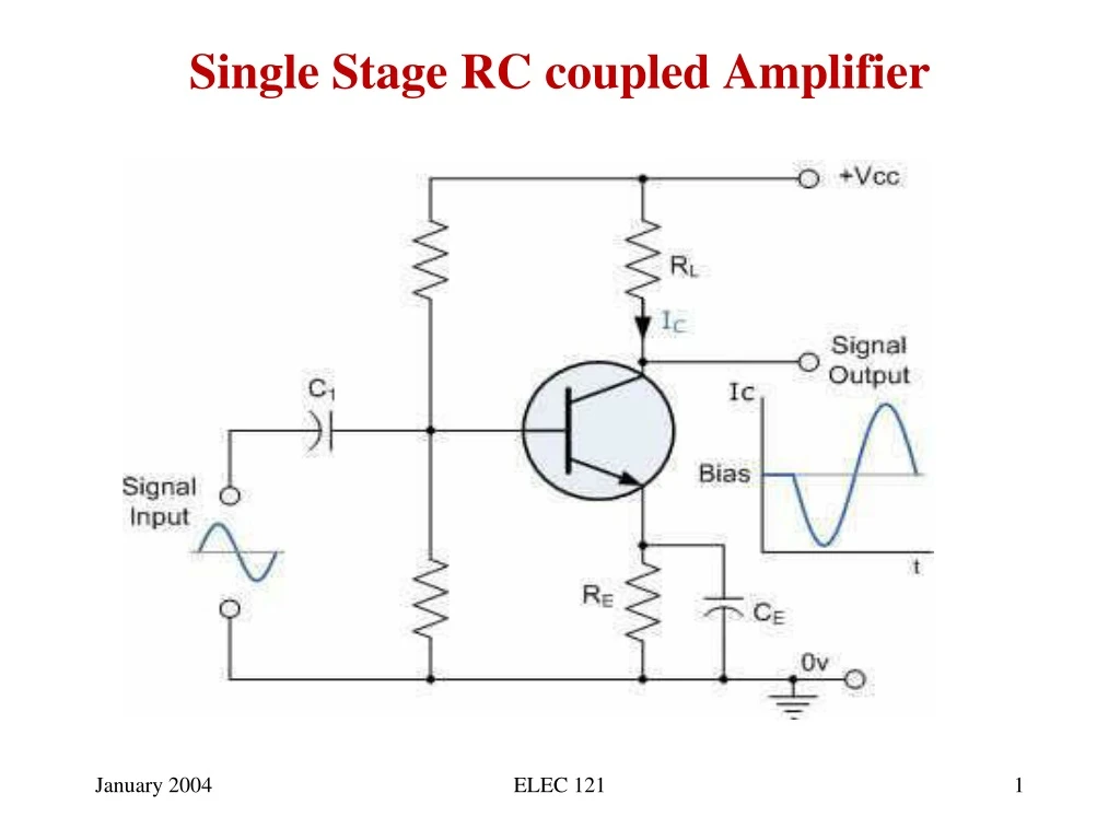
Single Stage RC coupled Amplifier ELEC 121
Frequency Response ELEC 121
Two Stage RC coupled amplifier ELEC 121
Frequency Response ELEC 121
JFET Construction There are two types of JFET’s: n-channel and p-channel. The n-channel is more widely used. There are three terminals: Drain (D) and Source (S) are connected to n-channel Gate (G) is connected to the p-type material ELEC 121
N-Channel JFET Operation The nonconductive depletion region becomes thicker with increased reverse bias. (Note: The two gate regions of each FET are connected to each other.) ELEC 121
Transfer (Transconductance) Curve From this graph it is easy to determine the value of ID for a given value of VGS It is also possible to determine IDSS and VP by looking at the knee where VGS is 0 ELEC 121
p-Channel JFET’s p-Channel JFET operates in a similar manner as the n-channel JFET except the voltage polarities and current directions are reversed ELEC 121
P-Channel JFET Characteristics • As VGS increases more positively • the depletion zone increases • ID decreases (ID < IDSS) • eventually ID = 0A • Also note that at high levels of VDS the JFET reaches a breakdown situation. ID increases uncontrollably if VDS > VDSmax. ELEC 121
Case Construction and Terminal Identification This information is found on the specification sheet ELEC 121
MOSFETs • MOSFETs have characteristics similar to JFETs and additional characteristics that make then very useful • There are 2 types of MOSFET’s: • Depletion mode MOSFET (D-MOSFET) • Operates in Depletion mode the same way as a JFET when VGS 0 • Operates in Enhancement mode like E-MOSFET when VGS > 0 • Enhancement Mode MOSFET (E-MOSFET) • Operates in Enhancement mode • IDSS = 0 until VGS > VT (threshold voltage) ELEC 121
MOSFET Handling MOSFETs are very static sensitive. Because of the very thin SiO2 layer between the external terminals and the layers of the device, any small electrical discharge can stablish an unwanted conduction. Protection: • Always transport in a static sensitive bag • Always wear a static strap when handling MOSFETS • Apply voltage limiting devices between the Gate and Source, such as back-to- back Zeners to limit any transient voltage ELEC 121
Depletion Mode MOSFET Construction The Drain (D) and Source (S) leads connect to the to n-doped regions These N-doped regions are connected via an n-channel This n-channel is connected to the Gate (G) via a thin insulating layer of SiO2 The n-doped material lies on a p-doped substrate that may have an additional terminal connection called SS ELEC 121
Basic Operation A D-MOSFET may be biased to operate in two modes: the Depletion mode or the Enhancement mode ELEC 121
p-Channel Depletion Mode MOSFET The p-channel Depletion mode MOSFET is similar to the n-channel except that the voltage polarities and current directions are reversed ELEC 121
n-Channel E-MOSFET showing channel length L and channel width W ELEC 121
Enhancement Mode MOSFET Construction The Drain (D) and Source (S) connect to the to n-doped regions These n-doped regions are not connected via an n-channel without an external voltage The Gate (G) connects to the p-doped substrate via a thin insulating layer of SiO2 The n-doped material lies on a p-doped substrate that may have an additional terminal connection called SS ELEC 121
How does a MOSFET work? No Voltage to Gate Voltage to Gate Source Drain Source Drain n n Simplified Notation No current flow “Short” allows current flow
Specification Sheet ELEC 121
E-MOSFET Symbols ELEC 121
Basic Operation The Enhancement mode MOSFET only operates in the enhancement mode. VGS is always positive IDSS = 0 when VGS < VT As VGS increases above VT, ID increases If VGS is kept constant and VDS is increased, then ID saturates (IDSS) The saturation level, VDSsat is reached. ELEC 121
Summary Table JFET D-MOSFET E-MOSFET ELEC 121