Download
1 / 9
90 likes | 99 Views
This paper proposes a implementation of a single phase transformer less photovoltaic inverter for grid connect PV system. We are developing new topology to eliminate the leakage current in which concept of charge pump circuit is introduced. In this paper, for controlling purpose we are utilizing Fuzzy Logic Controller. The neutral of the grid is directly connected to the negative polarity of the PV panel that creates a constant common mode voltage and zero leakage current. During the negative cycle, the charge pump circuit generates the negative output voltage of the proposed inverter. Therefore, according to the proportional resonant control strategy is used to control the injected current. There are various advantages of the proposed inverter they are the neutral of the grid is directly connected to the negative terminal of the PV panel, so the leakage current is eliminated, its compact size low cost the used dc voltage of the proposed inverter is the same as the full bridge inverter unlike neutral point clamped NPC , active NPC, and half bridge inverters flexible grounding configuration capability of reactive power flow and high efficiency. By using simulation result we can verify the concept of the proposed inverter and its practical application in grid tied PV systems. Anil Tekale | Radharaman Saha | Pratik Ghutke | Swapna God "Implementation of Fuzzy Based Grid-Tied PV System for Single Phase Transformer less Inverter with Charge Pump Circuit Concept" Published in International Journal of Trend in Scientific Research and Development (ijtsrd), ISSN: 2456-6470, Volume-3 | Issue-4 , June 2019, URL: https://www.ijtsrd.com/papers/ijtsrd23583.pdf Paper URL: https://www.ijtsrd.com/engineering/electrical-engineering/23583/implementation-of-fuzzy-based-grid-tied-pv-system-for-single-phase-transformer-less-inverter-with-charge-pump-circuit-concept/anil-tekale<br>

E N D
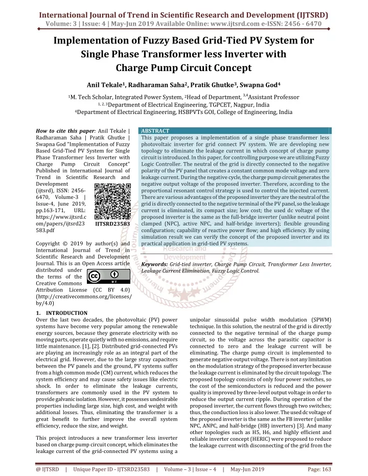
International Journal of Trend in Scientific Research and Development (IJTSRD) Volume: 3 | Issue: 4 | May-Jun 2019 Available Online: www.ijtsrd.com e-ISSN: 2456 - 6470 Implementation of Fuzzy Based Grid-Tied PV System for Single Phase Transformer less Inverter with Charge Pump Circuit Concept Anil Tekale1, Radharaman Saha2, Pratik Ghutke3, Swapna God4 1M. Tech Scholar, Integrated Power System, 2Head of Department,3,4Assistant Professor 1, 2, 3Department of Electrical Engineering, TGPCET, Nagpur, India 4Department of Electrical Engineering, HSBPVTs GOI, College of Engineering, India How to cite this paper: Anil Tekale | Radharaman Saha | Pratik Ghutke | Swapna God "Implementation of Fuzzy Based Grid-Tied PV System for Single Phase Transformer less Inverter with Charge Pump Circuit Concept" Published in International Journal of Trend in Scientific Research and Development (ijtsrd), ISSN: 2456- 6470, Volume-3 | Issue-4, June 2019, pp.163-171, URL: https://www.ijtsrd.c om/papers/ijtsrd23 583.pdf Copyright © 2019 by author(s) and International Journal of Trend in Scientific Research and Development Journal. This is an Open Access article distributed under the terms of the Creative Commons Attribution License (CC BY 4.0) (http://creativecommons.org/licenses/ by/4.0) 1.INTRODUCTION Over the last two decades, the photovoltaic (PV) power systems have become very popular among the renewable energy sources, because they generate electricity with no moving parts, operate quietly with no emissions, and require little maintenance. [1], [2]. Distributed grid-connected PVs are playing an increasingly role as an integral part of the electrical grid. However, due to the large stray capacitors between the PV panels and the ground, PV systems suffer from a high common mode (CM) current, which reduces the system efficiency and may cause safety issues like electric shock. In order to eliminate the leakage currents, transformers are commonly used in the PV system to provide galvanic isolation. However, it possesses undesirable properties including large size, high cost, and weight with additional losses. Thus, eliminating the transformer is a great benefit to further improve the overall system efficiency, reduce the size, and weight. ABSTRACT This paper proposes a implementation of a single phase transformer less photovoltaic inverter for grid connect PV system. We are developing new topology to eliminate the leakage current in which concept of charge pump circuit is introduced. In this paper, for controlling purpose we are utilizing Fuzzy Logic Controller. The neutral of the grid is directly connected to the negative polarity of the PV panel that creates a constant common mode voltage and zero leakage current. During the negative cycle, the charge pump circuit generates the negative output voltage of the proposed inverter. Therefore, according to the proportional resonant control strategy is used to control the injected current. There are various advantages of the proposed inverter they are the neutral of the grid is directly connected to the negative terminal of the PV panel, so the leakage current is eliminated, its compact size; low cost; the used dc voltage of the proposed inverter is the same as the full-bridge inverter (unlike neutral point clamped (NPC), active NPC, and half-bridge inverters); flexible grounding configuration; capability of reactive power flow; and high efficiency. By using simulation result we can verify the concept of the proposed inverter and its practical application in grid-tied PV systems. Keywords: Grid-tied inverter, Charge Pump Circuit, Transformer Less Inverter, Leakage Current Elimination, Fuzzy Logic Control. IJTSRD23583 unipolar sinusoidal pulse width modulation (SPWM) technique. In this solution, the neutral of the grid is directly connected to the negative terminal of the charge pump circuit, so the voltage across the parasitic capacitor is connected to zero and the leakage current will be eliminating. The charge pump circuit is implemented to generate negative output voltage. There is not any limitation on the modulation strategy of the proposed inverter because the leakage current is eliminated by the circuit topology. The proposed topology consists of only four power switches, so the cost of the semiconductors is reduced and the power quality is improved by three-level output voltage in order to reduce the output current ripple. During operation of the proposed inverter, the current flows through two switches; thus, the conduction loss is also lower. The used dc voltage of the proposed inverter is the same as the FB inverter (unlike NPC, ANPC, and half-bridge (HB) inverters) [3]. And many other topologies such as H5, H6, and highly efficient and reliable inverter concept (HERIC) were proposed to reduce the leakage current with disconnecting of the grid from the This project introduces a new transformer less inverter based on charge pump circuit concept, which eliminates the leakage current of the grid-connected PV systems using a @ IJTSRD | Unique Paper ID - IJTSRD23583 | Volume – 3 | Issue – 4 | May-Jun 2019 Page: 163
International Journal of Trend in Scientific Research and Development (IJTSRD) @ www.ijtsrd.com eISSN: 2456-6470 PV during the freewheeling modes [4]. The proposed inverter is capable of delivering reactive power into grid too. Fig. 1 illustrates a single-phase grid-tied transformer less inverter with CM current path, where P and N are the positive and negative terminals of the PV, respectively. The leakage current (iLeakage) flows through a parasitic capacitor (CP) between the filters (L1 and L2), the inverter, grid, and ground impedance (zg). This leakage current may cause safety problems, reduce the quality of injection current to the grid, as well as decrease the system efficiency [5]. (a) As shown in Fig. 2(b), the HERIC topology needs two extra switches on the ac side to decouple the ac side from the PV module in the zero stage. HERIC combines the merits of unipolar and bipolar modulation. Fig. 1. Block diagram of a single-phase grid-connected transformer less inverter with a leakage current path. In order to eliminate the leakage current, the CM voltage (CMV) (vcm) must be kept constant during all operation modes according to [6]. The vcm with two filter inductors (L1, L2) is calculated as follows: ( ( 2 2 L Where, VAn and VBn are the voltage differences between the midpoints A and B of the inverter to the dc bus minus terminal N, respectively. If L1 = L2 (asymmetrical inductor), vcm is calculated according to (1) and the leakage current appears due to a varying CMV. If L1 = L2 (symmetrical inductor), vcm is simplified to V V V Constant = = (b) Another solution to eliminate the leakage current is the direct connection of the negative PV terminal to the neutral point of the grid, such as the virtual dc-bus inverter and the unusual topology, as shown in Fig. 2(c), the virtual dc-bus inverter is composed of five insulated-gate bipolar transistors (IGBTs), two capacitors, and one filter inductor Lf. )( + ) − − + V V L L L V V 1 2 An Bn An Bn = + V (1) cm ) 1 2 + An Bn (2) cm 2 In this state, the CMV is constant and the leakage current is eliminated. In some structures such as the virtual dc-bus inverter [7] and NPC inverter, one of the filter inductors is zero and only one filter inductor is used. In this state, after simplification of vcm, it will have a constant value according to (3) and the leakage current will be eliminated ( ) 2 2 Then, ( ) 2 2 As shown in Fig. 2, there are various transformer less grid connected inverters based on the FB inverter in the literature to overcome these problems. The H5 inverter that is a FB-based inverter topology, compared to the conventional FB inverter, needs one additional switch (S5) on the dc side to decouple the dc side from the grid as shown in Fig. 2(a). (c) The virtual dc-bus generates the negative output voltage. The main drawback of this topology is that there is no path to charge the capacitor C2 during the negative cycle and this will cause a high output total harmonic distortion (THD). The topology presented, which is shown in Fig. 2(d), has a common ground with the grid. − + V V V V ( ) An Bn An Bn = + = = 0 V Constant L 1 cm − + V V V V An Bn ( ) An Bn = − = = 0 (3) V Constant L 1 cm (d) Fig.2. Single-phase grid-tied transformer less PV inverter topologies: (a) H5 inverter, (b) HERIC inverter, (c) virtual dc-bus inverter and (d) CM inverter proposed @ IJTSRD | Unique Paper ID - IJTSRD23583 | Volume – 3 | Issue – 4 | May-Jun 2019 Page: 164
International Journal of Trend in Scientific Research and Development (IJTSRD) @ www.ijtsrd.com eISSN: 2456-6470 The number of semiconductors used in this topology is low. However, the output voltage of this inverter is only two levels including positive and negative voltages without creating the zero voltage, which requires a large output inductor L2 and a filter. The inductor medium-type inverter also called “Karschny” is another topology that is derived from the buck–boost topology. This paper introduces a new transformer less inverter based on charge pump circuit concept, which eliminates the leakage current of the grid-connected PV systems using a unipolar sinusoidal pulse width modulation (SPWM) technique. The proposed topology consists of only four power switches, so the cost of the semiconductors is reduced and the power quality is improved by three-level output voltage in order to reduce the output current ripple. 2.Proposed Topology and Modulation Strategy 2.1.Charge Pump Circuit Concept The concept of a simple charge pump circuit to be used in the proposed topology to generate the inverter negative output voltage is shown in Fig. 3. The circuit consists of two diodes (D1, D2) and two capacitors (C1, C2). The capacitor C1 is used to couple the voltage point of A to the node D. Two Schottky diodes D1 and D2 are used to pump the output voltage. In steady state, the output voltage of the negative charge pump circuit (vCn) can be derived by V V V V − − = − + + Where, Vdc is the input voltage, Vcut−in−D1 and Vcut−in−D2 are the cut-in voltages of the diodes D1 and D2, respectively. For high power applications, these values can be negligible. 2.2.Proposed Methodology As shown in Fig. 4, the proposed topology consists of four power switches (S1 − S4), two diodes (D1, D2), two capacitors (C1, C2) based on the charge pump circuit as described in Section 2.1. Fig.4. Proposed single-phase transformer less grid- connected inverter This new topology is modulated using simple SPWM. Fig. 5 shows the gate drive signals for the proposed inverter under the current lagging condition. According to the direction of the inverter output voltage and output current, the operation of the proposed inverter is divided in four regions as shown in Fig. 6. (4) − − cm dc cut in D cut in D 1 2 Fig.5. Switching pattern of the proposed topology with reactive power flow Region I: The inverter output voltage and the output current are positive; energy is transferred from dc side to grid side as shown in Fig. 6(a). Fig.3. Schematic diagram of the proposed inverter including the charge pump circuit. The above principle is integrated into the proposed inverter by using additional switching devices. In summary, the charge pump circuit in the transformer less inverter has the following characteristics for grid-tied applications. 1.This circuit has a common line with the negative terminal of the input dc voltage and the neutral point of the grid that causes the leakage current to be eliminated. 2.The charge pump circuit has no active device and it has a lower cost for grid-tied applications. (a) @ IJTSRD | Unique Paper ID - IJTSRD23583 | Volume – 3 | Issue – 4 | May-Jun 2019 Page: 165
International Journal of Trend in Scientific Research and Development (IJTSRD) @ www.ijtsrd.com eISSN: 2456-6470 When the switches S1 and S2 are ON, the output voltage of the inverter (vAn) will be +Vdc (positive state) as shown in Fig. 6(a) and (g). During this time interval, diode D1 is reverse biased and D2 is ON, so the capacitor C1 is charged through diode D2 and the voltage across the capacitor C2 maintains to be constant. In this state, when the switches S2 and S3 are ON, vAn will be 0 (zero state) as shown in Fig. 6(b) and (h). (b) Region II: The inverter output voltage is negative and the output current is positive; energy is transferred from grid side to dc link as shown in Fig. 6(c). (g) (c) (h) Fig :6 Operational stages of the proposed inverter during (a), (b) region I, (c), (d) region II, (e), (f) Region III and (g), (h) region IV (?) ???= +???, ??>0. (?) ???=0, ??>0. (?) ???=−???, ??>0. (?) ???=0, ??>0. (?) ???=−???, ??<0. (?) ???=0, ??<0. (?) ???= +???, ??<0. (h) ???=0, ??<0. In the regions II and III, the negative and zero voltage levels are produced. Fig. 6 (c) and (e) shows the equivalent circuit that S4 and S1 are ON. The negative voltage is generated, when switch S4 is turned ON and the voltage across the capacitor C2 appears at the inverter output voltage (vAn = −Vdc) (negative state). The voltage across the capacitor C1 can be kept constant in this state by the modulation strategy. In this period, the circuit operation of the zero state is similar to the zero state of positive half-period of the grid as shown in Fig. 6 (b) and (h). In this case, the charging time constant of capacitor C2 (τC2) can be expressed as follows: R C e C τ = The current through capacitors (icapacitors) is calculated by eV i C τ According to (5), the charging time constant of C2 is larger than its natural discharging time constant and VC1− VC2 has a very small value in steady state. 3.Analysis of the Proposed Topology 3.1.Current Stress Analysis and Capacitor Design In this section, current stress analysis of the proposed topology has been presented. As capacitor C1 is charged (d) Region III: the inverter output voltage and the output current are negative; energy is transferred from dc link to grid side as shown in Fig. 6(e). Region IV: the inverter output voltage is positive and the output current is negative; energy is transferred from grid side to dc side as shown in Fig. 6(g) (5) 2 e1 1 (e) − V 1 2 C C = (6) 1 C apacitors 2 C (f) @ IJTSRD | Unique Paper ID - IJTSRD23583 | Volume – 3 | Issue – 4 | May-Jun 2019 Page: 166
International Journal of Trend in Scientific Research and Development (IJTSRD) @ www.ijtsrd.com eISSN: 2456-6470 − through switch S1 and capacitor C2 is charged through switch S3, the maximum value of the current stress occurs on the switches S1 & S3. Simulation results of the current in the switches S1 & S3 for an output power of 500 W are shown in Fig. 7. The selected parameters of the simulations are the same as the simulation 500 W prototype. These parameters are listed in Table IV. The maximum value of the current in these switches occurs at the negative state in simulation results as shown in Fig. 7. In the negative half-period of the grid, the circuit shifts between the negative and zero states. During the negative state, the capacitor C1 is charged by the capacitor CB, while the capacitor C2 is discharged by the grid. dv I C v R i R C , 2 ,1 + diff dt pv diff s g 3 = − (8) (R ) e1 3 1 B s According to Fig.8 (b), at the zero state dv R I dt R dv dt Where in (8) -(11), Re2 and Ce2 will be as follows: dv i + ,1 , 2 diff Cb pv diff g = + (9) + ( R ) C C v e 2 R I 1 2 cb − I C , 2 ,1 diff pv cb PV diff = + (10) R C e 2 2 B e C C C 1 + B = + + + = R , R R R R C (11) e 2 2 1 1 2 D s C CB e C 1 B By using the averaging method at the switching cycle Ts, and linearizing (8) – (11), the average value of iS1 and iS3 at the negative and zero states is equal to (13) and (14), respectively: dv v R i s t dt C + dv I v R i st dt C + − + CB PV R I R I st v ,1 ,1 3 ,2 diff diff s g diff = + − + (1 ( )) ( )( s t ) iC 2 g + (R R ) ( R ) C e1 e2 1 e2 R I 1 e CB − + v ,2 ,1 3 ,2 ) diff PV diff s g C PV C CB PV diff (1 ())( = + − − + ) ()( ) + (R R ) (R C e1 e2 1 e2 e2 (12) B B Fig:7 Simulations of the current of switches: (a) grid current (ig) [1 A/div], (b) (is1) [2 A/div], (c) (is3) [2 A/div]. where s(t) denotes the switching state function given as follows: 1 when the circuit is at positive state 0 when the circuit is at zero state 1 when the circuit is at negative state The average current of iS1 and iS3 during Ts can be found as follows: v T R i T R + v T R i T = Therefore, the voltage difference between the capacitors C1 and CB as well as the capacitors C1 and C2 is decreased. The equivalent circuits of the zero and negative states of the proposed topology for the current stress analysis are shown in Fig. 8(a) and (b), respectively. According to the electric circuit theory, the grid voltage in series with a grid-side inductor (Lg) can be equivalent with the current source (ig) as shown in Fig. 8. − ( ) s t = = i T ,1 3 diff s S g s = (13) 1 2 s R e 1 3 s = CB PV I , 2 diff s (14) 1 2 s R e 2 The simulation results of the current flowing through the switches S1 and S3 for the output power 500 W are shown in Fig. 7. The value of the current that passes through S1 and S3 to reach to its maximum at the negative state is shown in this figure too. At the negative state, 1 1 2 1 C C + − 1 1 2 1 B C C + Equations (22) and (23) indicate that the values of C1/ (C1 + C2) and C1/ (C1 + CB) should be calculated small enough, and the values of the Re1Ce1 and Re2Ce2 should be smaller than the switching period in order to minimize the current stress on the switches. These values can be limited by a small resistor or a small inductor between the capacitors if needed. The relationship between the voltage and current passing through the capacitors is calculated by (a) − I M I M 1 C M T M 1 m s C = + + 1,max s i T (15) R 2 − 1 2 e1 T 1 e 1 C M − M 1 m s C = + + 3,max s i T (16) R 2 1 e2 2 e (b) Fig.8. Equivalent circuit of the proposed converter during zero state and (b) negative state According to Fig.8 (a), at the zero state dv v dt R C + − R i ,1 ,1 diff diff s g 3 = (7) (R ) e1 3 1 s e @ IJTSRD | Unique Paper ID - IJTSRD23583 | Volume – 3 | Issue – 4 | May-Jun 2019 Page: 167
International Journal of Trend in Scientific Research and Development (IJTSRD) @ www.ijtsrd.com eISSN: 2456-6470 ∆ = ∆ II. The switching losses of the MOSFET switch can be found as follows: Table II: Specifications and Power Devices for Efficiency Evaluation Parameter Input Voltage Grid Voltage/Frequency 220 V/50 Hz Rated Power AC Output Current Switching Frequency Duty Ration (M) P f E = where Eoss is the stored energy that can be achieved from the datasheet that is equal to 45 μJ. The total switching losses of the switches in the proposed inverter can be derived as follows: 4 Total SW SW OSS P f E V = 3.3.Conduction Losses in the Capacitors The ESR of the capacitors of the proposed inverter is achieved from aluminium electrolyte capacitor datasheets and it is divided into two parts. The second part of the conduction losses is related to the inrush current during the charging of the capacitors. These losses can be defined as follows: 2( C CB CAP Cond P π 2( C C CAP Cond P π where dc(t) is the duty ratio of the capacitor. 3.4.Control Scheme The control strategy of the proposed grid-tied single-phase inverter is shown in Fig. 9. It contains two cascaded loops [21]: the first loop is an inner control loop, which has the responsibilities to generate a sinusoidal current and the outer control loop is implemented for the current reference generation, where the power is controlled. The transfer function of this controller can be found as follows: c v t i C (17) C The required capacitance of C1 and CB for the proposed inverter can be derived by equalling the capacitor power magnitude to the grid power ripple magnitude. The capacitance C1 and CB can be calculated as follows: ( ( V V f ∧ where IC1max and ICBmax are the maximum current that passes through the capacitors C1 and CB, respectively. ∧Vr, Vn, and f are the capacitor voltage ripple magnitude, nominal voltage on the capacitor, and the frequency during maximum current, respectively. 3.2.Conduction and Switching Losses of Power Devices During the positive power cycle, the grid current flows through switches S1 and S2 and the capacitor C1 is charged through diode D2 at the positive state as shown in Fig. 6(a) and (g). The capacitor C1 is charged through diode D2 and switch S1 at the negative state as shown in Fig. 6(c) and (e). The voltage drop of the power devices can be derived by ( ) MOSFET: v t i t R = ( ) Diode: v t V i t R = + where VDS is the drain source voltage drop of the MOSFET, RDS is the drain source resistance of the MOSFET during on the state operation, VAK is the anode cathode voltage drop of the diode, VF is the equivalent voltage drop under zero current condition of the diode, RAK is the anode cathode resistance of the diode during the on state, and i(t) is the grid current. The average value of the conduction losses of the MOSFET switch (PMOSFET Cond) during half of the fundamental period is calculated by 1 MOSFET Cond DS P v t i t d π Table I: Duty Ratio of Each Conducting Device Value 400 V ) orB max I 1 C 500 W 2.3 A 24 KHz 0.78 or B= C (18) 1 ) r n V (23) _ MOSFET SW SW OSS F = 3.46 W (24) _ F ( ) ( ) (19) DS DS (20) F AK AK π ∫ + ) R R ( ) ( ) t d t 1 = ω 2 s d t i (25) _ _ 1 c 1 0 π ∫ + ) R R ( ) ( ) t d t 1 2 ω = 2 s d t i (26) _ _ 2 c 3 0 π ( ) ( ) ( ) t d t = ∫ ω (21) _ MOSFET 0 Duty ratio (d) Positive cycle (vg>0) Negative Cycle (vg<0) sin M t ω 1 sin M t ω 1- 0 0 sin M t ω Semiconductor Devices ω ω ω t ω t ω sin sin M sin M sin M sin M M t S1 S2 S3 S4 D1 D2 t t 1- 0 The average value of the conduction loss in the diode (PDiode_Cond) during the on state mode is calculated by 1 AK Diode Cond P v i t d π π ( ) ( ) t d t = ∫ ω _ Diodes 0 π 1 π ( ) ( ) ( ) t d t = ∫ ω v i t R i t d (22) Diodes F AK 0 The device manufacturer and circuit parameters for efficiency evaluation of proposed inverter are listed in Table Fig.9. Control block diagram of the proposed single-phase grid-tie inverter based on single-phase PQ theory @ IJTSRD | Unique Paper ID - IJTSRD23583 | Volume – 3 | Issue – 4 | May-Jun 2019 Page: 168
International Journal of Trend in Scientific Research and Development (IJTSRD) @ www.ijtsrd.com eISSN: 2456-6470 Lg=rLf 4.Fuzzy Logic Controller In FLC, basic control action is determined by a set of linguistic rules. These rules are determined by the system. Since the numerical variables are converted into linguistic variables, mathematical modelling of the system is not required in FC. The FLC comprises of three parts: Fuzzification, interference engine and Defuzzification. The FC is characterized as 1.Seven fuzzy sets for each input and output. 2.Triangular membership functions for simplicity. (35) 2 K + r = + G K (27) ( ) PR s p ω 2 2 s where kp is the proportional gain, kr is the fundamental resonant gain, and ω is the resonant frequency. According to the single-phase PQ theory the current reference can be produced by regulating the active and reactive powers. The active power (P) and reactive power (Q) for the proposed topology can be calculated by v i v i P = , Q = ga ga v i v i + β β − β β ga ga g g g g (28) 2 2 where vgα, vgβ, igα, and igβ are the α and β components of grid voltage and current, respectively. The active power and reactive power references (P∗ and Q∗) can be tuned by the operators {R– 3} or in the control unit, when the MPPT control is activated. If PI controllers are used for power regulations, the grid current reference (ig-ref) can be derived as follows [24]: * P P − ( ) ( ) Gp s Fig.10. Fuzzy logic controller 1 [ ] = ( ) i v v (29) − β g ref ga g 2 2 * v v − β Q Q − ga g ( ) ( ) Gq s 3.Fuzzification using continuous universe of discourse. 4.Implication using Mamdani’s ‘min’ operator. 5.Defuzzification using the height method. Table III: Fuzzy Rules where Gp(s) and Gq(s) are the PI controllers for active power and reactive power, respectively. The LCL filter is adopted as the grid interfaced filter in this proposed topology. High output current quality in the proposed inverter can be obtained if the output filter is configured correctly. The inverter-side inductor (Lf) value is calculated by considering 10–20% of the ripple on the output current, which is given by ( sin f SW L f i ∆ where fsw is the switching frequency and ΔiL represents the peak-to-peak ripple current on the Lf. The inverter output volt age (vAn) can be calculated as follows: sin An dc v MV t ω = By replacing (39) with (38) and simplifying it, we have ( f SW L f i ∆ where RF is the ripple current and can be calculated from 2 2 sin sin RF M t M ω = − The maximum achievable value of modulation index (M) is RFmax = 0.25 [26]. The maximum value of the filter capacitor is calculated by (42), limiting to be less than 5% of the nominal value [27] 0.05 2 rms fV π where Pn is the nominal power, Vrms denotes the root mean square (RMS) grid voltage, and f presents the grid frequency. There is a relation between the inverter-side inductor (Lf) and the grid side (Lg). This value is determined with the ratio between the ripple attenuation (r) as described in [28] )( ) − ω v v M t dc An = L (30) ?Fuzzification: Membership function values are assigned to the linguistic variables, using seven fuzzy subsets: NB (Negative Big), NM (Negative Medium), NS (Negative Small), ZE (Zero), PS (Positive Small), PM (Positive Medium), and PB (Positive Big). The input error for the FLC is given as ( ) ( ) ph k ph k-1 V -V ( ) CE k E k E k-1 = − ?Inference Method: Several composition methods such as Max–Min and Max-Dot have been proposed in the literature. In this paper Min method is used. The output membership function of each rule is given by the minimum operator and maximum operator. Table 1 shows rule base of the FLC. ?Defuzzification: As a plant usually requires a non-fuzzy value of control, a Defuzzification stage is needed. To compute the output of the FLC, “height‟ method is used and the FLC output modifies the control output. Further, the output of FLC controls the switch in the inverter. (31) )( ) v RF dc = L (32) ( ) ( ) ph k P -P ph k-1 = E k (36) ( ) ω t (33) ( ) ( ) (37) P n = C (34) , max F 2 @ IJTSRD | Unique Paper ID - IJTSRD23583 | Volume – 3 | Issue – 4 | May-Jun 2019 Page: 169
International Journal of Trend in Scientific Research and Development (IJTSRD) @ www.ijtsrd.com eISSN: 2456-6470 To achieve this, the membership functions of FC are: 1.Error 2.Change in error 3.Output The set of FC rules are derived from ( 1 u E α α = − = − ) ∗ C (38) Fig.11. input error as membership functions Fig.14. simulation block diagram of proposed single-phase transformer less grid-connected inverter From Fig. 15, it is clear that the output current and voltage of the proposed inverter are highly sinusoidal with low harmonic distortion due to the three-level inherency of the output voltage. The current harmonic distribution is demonstrated in Fig. 10. Fig.12. Change as error membership functions Fig. 15 Simulation results of the proposed topology (a) Grid Voltage (b) Grid Current (c) Inverter Voltage Fig.13. Output variable membership functions It is clear that the pulse duration of the output voltage (vAn) is in agreement with the switching frequency. The voltage stress of the capacitors and diodes is shown in Fig. 16. Where α is self-adjustable factor which can regulate the whole operation. E is the error of the system; C is control variable. 5.Simulation Results In fig 14 the proposed grid connected inverter has been presented. The simulation results of the proposed grid- connected inverter operation are presented in Fig 15. Table IV Parameters for the 500 W Prototype Fig. 16 Simulation results of the capacitor and diode voltages (a) Capacitor Voltage (b) Diode Voltage Simulation results for drain source voltage of switches are shown in Fig. 17 @ IJTSRD | Unique Paper ID - IJTSRD23583 | Volume – 3 | Issue – 4 | May-Jun 2019 Page: 170
International Journal of Trend in Scientific Research and Development (IJTSRD) @ www.ijtsrd.com eISSN: 2456-6470 [3]T. Bruckner, S. Bernet, and H. Guldner, “The active NPC converter and ¨ its loss-balancing control,” IEEE Trans. Ind. Electron., vol. 52, no. 3, pp. 855–868, Jun. 2005. [4]Swapna Popat God, Anil Tekale, Mallareddy C., “Control Scheme based on Quasi Z-Source Network for Four Switch Three Phase Brushless DC Motor”, in IJSRD, vol.5, issue 07, ISSN-2321-0613, page. No. 461-462, June 2017. [5]D. Barater, E. Lorenzani, C. Concari, G. Franceschini, and G. Buticchi, “Recent advances in single-phase transformer less photovoltaic inverters,” IET Renewable Power Generation, vol. 10, no. 2, pp. 260–273, 2016. [6]B. Yang, W. Li, Y. Gu, W. Cui, and X. He, “Improved transformer less inverter with common-mode leakage current elimination for a photovoltaic grid connected power system,” IEEE Trans. Power Electron., vol. 27, no. 2, pp. 752–762, Feb. 2012. Fig. 17 Simulation results of the Switches (a) Vs1 (b) Vs2 (c) Vs3 (d)Vs4 6.Conclusion In this paper we are implementing a new single-phase transformer less inverter for a grid-tied PV system using a charge pump circuit concept with the fuzzy controller. Therefore, the main concept of the proposed system is to generate the negative output voltages which have been developed in this proposed inverter. Here we are using the fuzzy logic controller for the better performance because the fuzzy controller is the most suitable for the human decision- making mechanism, providing the operation of an electronic system with decisions of experts. Therefore, we are developing the proposed topology which is similar to the neutral line in the grid; therefore, the leakage current will be suppressed and the transformer is eliminated. Moreover, the proposed topologies have the capability to deliver the required reactive power into the grid. Therefore, the proposed topology is used to realize the minimum number of components and higher power density can be achieved with lower design cost. By using the simulation result we can verify the proposed system. References [1]S. B. Kjaer, J. K. Pedersen, and F. Blaabjerg, “A review of single-phase grid connected inverters for photovoltaic modules,” IEEE Trans. Ind. Electron., vol. 41, no. 5, pp. 1292–1306, Sep./Oct. 2005. [7]F. Bradaschia, M. C. Cavalcanti, P. E. P. Ferraz, F. A. S. Neves, E. C. Santos, and J. H. G. M. da Silva, “Modulation for three-phase transformer less z-source inverter to reduce leakage currents in photovoltaic systems,” IEEE Trans. Ind. Electron., vol. 58, no. 12, pp. 5385–5395, Dec. 2011. [8]Y. Gu, W. Li, Y. Zhao, B. Yang, C. Li, and X. He, “Transformer less inverter with virtual dc bus concept for cost-effective grid-connected PV power systems,” IEEE Trans. Power Electron., vol. 28, no. 2, pp. 793– 805, Feb. 2013. [9]W.-J. Cha, K.-T. Kim, Y.-W. Cho, S.-H. Lee, and B.-H. Kwon, “Evaluation and analysis of transformer less photovoltaic inverter improvement and reduction of leakage current,” IET Power Electron., vol. 8, no. 2, pp. 255–267, 2015. topology for efficiency [10]H. Xiao and S. Xie, “Leakage current analytical model and application in single-phase transformer less photovoltaic grid-connected inverter,” IEEE Trans. Electromagnetic Compat., vol. 52, no. 4, pp. 902–913, Nov. 2010. [11]W. Yu et al., “High-efficiency inverter with H6-type configuration for photovoltaic non-isolated ac module applications,” in Proceeding. Annual. IEEE Appl. Power Electron. Conf. Expo., 2010, pp. 1056–1061. [2]X. Guo, R. He, J. Jian, Z. Lu, X. Sun, and J. M. Guerrero, “Leakage current elimination of four-leg inverter for transformer less three-phase PV systems,” IEEE Trans. Power Electron., vol. 31, no. 3, pp. 1841–1846, Mar. 2016. [12]Tekale Anil A, Ghule Puja R., “Switched DC Sources Based Novel Multilevel Inverter”, in IRJET, vol.4, issue.6, 2017, ISSN- 2395-0056, pp. 123-127. @ IJTSRD | Unique Paper ID - IJTSRD23583 | Volume – 3 | Issue – 4 | May-Jun 2019 Page: 171