Download
1 / 33
340 likes | 746 Views
FPGA Architecture. Tsung-Yi Wu. Topics. Designer’s Choice FPGA Architecture Example: Spartan-II Architecture Xilinx vs. Altera. Designer ’ s Choice. SSI (small scale integrated circuits) or MSI (medium scale integrated circuits) components Difficulties arises as design size increases

E N D
FPGA Architecture Tsung-Yi Wu
Topics • Designer’s Choice • FPGA Architecture • Example: Spartan-II Architecture • Xilinx vs. Altera
Designer’s Choice • SSI (small scale integrated circuits) or MSI (medium scale integrated circuits) components • Difficulties arises as design size increases • Interconnections grow with complexity resulting in a prolonged testing phase • Simple programmable logic devices • PALs (programmable array logic) • PLAs (programmable logic array) • Architecture not scalable; Power consumption and delays play an important role in extending the architecture to complex designs • Implementation of larger designs leads to same difficulty as that of discrete components
Designer’s Choice • PAL/PAL
In1 Out1 "0" In2 Out2 In3 "0" Out3 In4 "0" Designer’s Choice • PAL
In1 Out1 In2 "0" Out2 In3 "0" Out3 In4 "0" Designer’s Choice • PAL Out1 = (In1 & In2’ & In3+ In1')'
Designer’s Choice • PLA
Designer’s Choice • FPGA (Field Programmable Logic Devices) • Customized by end user • Implements multi-level logic function • Fast time to market and low risk • Channel Based Routing • Post Layout Timing
Designer’s Choice • CPLD(Complex Programmable Logic Device) • Wide, Fast Complex Gating • Easily Routed • Central, Global Interconnect • Simple, Deterministic Timing • Routing 較 FPGA 簡單,延遲時間較短
Designer’s Choice • FPGA vs. CPLD
Designer’s Choice • ASIC
FPGA Architecture • Based on the principle of functional completeness • FPGA: Functionally complete elements (Logic Blocks) placed in an interconnect framework • Interconnection framework comprises of wire segments and switches; Provide a means to interconnect logic blocks • Circuits are partitioned to logic block size, mapped and routed
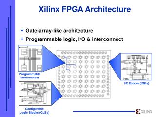
FPGA Architecture • IOB: Input/Output Blocks • CLB: Configurable Logic Blocks • Programmable Interconnections
FPGA Architecture • CLB
FPGA Architecture • Programmable Interconnections
FPGA Architecture • Programmable Interconnections
FPGA Architecture • Field Programmability • Achieve through switches (Transistors controlled by memory elements or fuses) • Switches control the following aspects • Interconnection among wire segments • Configuration of logic blocks • Distributed memory elements controlling the switches and configuration of logic blocks are together called “Configuration Memory”
FPGA Architecture • Technology of Programmable Elements • Vary from vendor to vendor. • All share the common property: Configurable in one of the two positions –‘ON’ or ‘OFF’ • Can be classified into three categories: • SRAM based • Fuse based • EPROM/EEPROM/Flash based • Desired properties: • Minimum area consumption • Low on resistance; High off resistance • Low parasitic capacitance to the attached wire • Reliability in volume production
FPGA Architecture • SRAM Programming Technology • Employs SRAM (Static RAM) cells to control pass transistors and/or transmission gates • SRAM cells control the configuration of logic block as well • Volatile • Needs an external storage • Needs a power-on configuration mechanism • In-circuit re-programmable • Lesser configuration time • Occupies relatively larger area
FPGA Architecture • SRAM Programming Technology
FPGA Architecture • An Example • Modulo-4 counter
FPGA Architecture • Modulo-4counter: LogicImplementation
FPGA Architecture • Modulo-4 counter: FPGA Implemen- tation
FPGA Architecture • FPGA vs. ASIC
Example: Spartan-II Architecture • Configurable logic blocks • Implement logic here! • I/O blocks • Communicate with other chips • Choose from 16 signal standards • Block RAM • On-chip memory for higher performance
Example: Spartan-II Architecture • Top-Level
Example: Spartan-II Architecture • Simplified • 1 CLB holds 2 slices • Each slice contains two sets of the following: • Four-input LUT • Any 4-input logic function • Or 16-bit x 1 RAM • Or 16-bit shift register
Example: Spartan-II Architecture • Each slice contains two sets of the following: • Carry & control • Fast arithmetic logic • Multiplier logic • Multiplexer logic • Storage element • Latch or flip-flop • Set and reset • True or inverted inputs • Sync. or async. control
CLB Slice MUXF6 MUXF5 Slice MUXF5 LUT LUT LUT LUT Example: Spartan-II Architecture • MUXF5 combines 2 LUTs to form • 4x1 multiplexer • Or any 5-input function • MUXF6 combines 2 slices to form • 8x1 multiplexer • Or any 6-input function
Example: Spartan-II Architecture • I/O Block (Simplified)
Xilinx vs. Altera • Altera Stratix • 1.5v 130nm copper • 114,140 logic elements • 10Mb RAM • 224 9x9 multipliers • No hard processor cores (Excalibur, based on Apex 20k) • Xilinx Virtex-II Pro • 1.5v 130nm copper • 125,136 logic cells • 10Mb RAM • 556 18x18 multipliers • Up to four PowerPC 405 cores
Xilinx vs. Altera • Altera Stratix
Xilinx vs. Altera • Xilinx Virtex-II Pro