Download
1 / 12
130 likes | 406 Views
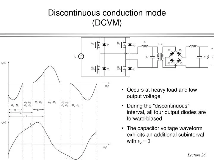
Discontinuous conduction mode (DCVM). Occurs at heavy load and low output voltage During the “discontinuous” interval, all four output diodes are forward-biased The capacitor voltage waveform exhibits an additional subinterval with v c = 0. State plane trajectory: DCVM.

E N D
Discontinuous conduction mode(DCVM) • Occurs at heavy load and low output voltage • During the “discontinuous” interval, all four output diodes are forward-biased • The capacitor voltage waveform exhibits an additional subinterval with vc = 0
State plane trajectory: DCVM As predicted by CCM analysis DCVM trajectory DCVM occurs when
DCVM solution Mode boundary Steady-state solution • Output characteristics • Solid lines: CCM • Dashed lines: DCVM
Design considerations • Let’s now consider how to design a resonant converter in a dc-dc converter application in which the output voltage V is to be regulated over a range of operating points. Typical specifications are of the form Pmax ≤ P ≤ Pmin Vgmax ≤ Vg ≤ Vgmin V is regulated • How specifications map into the converter output plane M = V / nVg J = nR0I / Vg • The turns ratio n can be chosen to map the range of voltage operating points to any valid range of M: Current and power are related to J: Hence
Peak tank capacitor voltage stressesProportional to output voltage in CCM Peak capacitor voltage, CCM: DCVM: (above equations are derived from the state plane trajectory) (the course notes include Fig. 5.26(b) that shows peak voltage stresses below the peak frequency in the double frequency region)
Peak current stressesProportional to output voltage in CCM Peak transistor current, CCM: DCVM: (above equations are derived from the state plane trajectory) (the course notes include Fig. 5.25(b) that shows peak current stresses below the peak frequency in the double frequency region)
Design exampleOff-line dc-dc converter Design a dc-dc converter using a parallel resonant converter, to meet the following specifications: It is desired to operate MOSFET devices with zero-voltage switching
Choice of range of operating points Here, “converter design” involves selection of a valid range of M and J, that is mapped into the range of converter specifications through selection of the turns ratio and characteristic impedance according to The values of L and C are then chosen as follows:
A D B C One possible design Corners of the operating region for the design Mmax = 1.2, Jmax = 0.9 Operating region overlayed on the converter output characteristics
1 2 3 5 • • • • Comparison of some other choices Choose Mmax, Jmax close to the boundary of allowed operation to minimize peak current stress Increasing Mmax leads to operation closer to resonance, with reduced range of switching frequencies