Download
1 / 26
260 likes | 462 Views
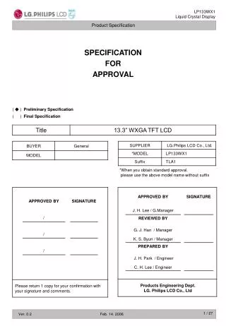
SPECIFICATION FOR APPROVAL. APPROVED BY. Signature. J. H. Lee / S.Manager. REVIEWED BY. K.K.Jang / Manager. PREPARED BY. N.J. Seong / Engineer. Product Engineering Dept. LG. Philips LCD Co., Ltd. No. ITEM. Page. COVER. 1,2. CONTENTS. 3. RECORD OF REVISIONS. 4. 1.

E N D
SPECIFICATION FOR APPROVAL APPROVED BY Signature J. H. Lee / S.Manager REVIEWED BY K.K.Jang / Manager PREPARED BY N.J. Seong / Engineer Product Engineering Dept. LG. Philips LCD Co., Ltd
No ITEM Page COVER 1,2 CONTENTS 3 RECORD OF REVISIONS 4 1 GENERAL DESCRIPTION 5 2 ABSOLUTE MAXIMUM RATINGS 6 3 ELECTRICAL SPECIFICATIONS 7 3-1 ELECTRICAL CHARACTREISTICS 6 3-2 INTERFACE CONNECTIONS 9 3-3 SIGNAL TIMING SPECIFICATIONS 10 3-4 SIGNAL TIMING WAVEFORMS 10 3-5 COLOR INPUT DATA REFERNECE 11 3-6 POWER SEQUENCE 12 4 OPTICAL SFECIFICATIONS 13 5 MECHANICAL CHARACTERISTICS 17 6 RELIABLITY 21 7 INTERNATIONAL STANDARDS 22 7-1 SAFETY 22 7-2 EMC 22 8 PACKING 23 8-1 DESIGNATION OF LOT MARK 23 8-2 PACKING FORM 23 9 PRECAUTIONS 24 MOUNTING PRECAUTIONS 24 9-1 9-2 OPERATING PRECAUTIONS 24 9-3 ELECTROSTATIC DISCHARGE CONTROL 25 PRECAUTIONS FOR STRONG LIGHT EXPOSURE 25 9-4 9-5 STORAGE 25 9-6 HANDLING PRECAUTIONS FOR PROTECTION FILM 25 A APPENDIX. Enhanced Extended Display Identification Data 26 Contents
RECORD OF REVISIONS Revision No Revision Date Page Description Note 1.0 Jun. 16, 2005 - Final Specification
1. General Description The LP150E06 is a Color Active Matrix Liquid Crystal Display with an integral Cold Cathode Fluorescent Lamp(CCFL) backlight system. The matrix employs a-Si Thin Film Transistor as the active element. It is a transmissive type display operating in the normally white mode. This TFT-LCD has 15.0 inches diagonally measured active display area with SXGA+ resolution(1050 vertical by 1400 horizontal pixel array) Each pixel is divided into Red, Green and Blue sub-pixels or dots which are arranged in vertical stripes. Gray scale or the brightness of the sub-pixel color is determined with a 6-bit gray scale signal for each dot, thus, presenting a palette of more than 262,144 colors. The LP150E06 has been designed to apply the interface method that enables low power, high speed, low EMI. The LP150E06 is intended to support applications where thin thickness, low power are critical factors and graphic display are important. In combination with the vertical arrangement of the sub-pixels, the LP150E06 characteristics provide an excellent flat display for office automation products such as Notebook PC. Column Driver Circuit LVDS & Timing Control CN1 Block TFT-LCD Row Dirver Circuit (1400X1050) Power Block J1 Backlight Lamp Ass'y :Control & Data :Power General Features
90% 80% 60% 60 Wet Bulb Temperature [℃] 50 Humidity[(%)RH] Storage 40% 40 30 Operation 20 20% 10 0 10% -20 0 10 60 70 80 20 30 40 50 Dry Bulb Temperature [℃] 2. Absolute Maximum Ratings The following are maximum values which, if exceeded, may cause faulty operation or damage to the unit. Table 1. ABSOLUTE MAXIMUM RATINGS Parameter Symbol Values Units Notes Min Max Power Input Voltage-ON VCC 2.7 4.0 Vdc at 25 5C Power Input Voltage-OFF GND -0.3 0.3 Vdc at 25 5C Operating Temperature TOP 0 50 C 1 Storage Temperature TST -20 60 C 1 Operating Ambient Humidity HOP 10 90 %RH 1 Storage Humidity HST 10 90 %RH 1 Electrostatic Durability (ESD) VESD ± 8.0 kV 2 Note : 1. Temperature and relative humidity range are shown in the figure below. Wet bulb temperature should be 39C Max, and no condensation of water. 2. Condition 1) Non-operation, 150㎊-330Ω, 25℃, 40~60%RH 2) I/F Connector pins are subjected. 3) The surface of Metal bezel and LCD are subjected except interface connector.(LCD side) 4) Discharge interval time 1sec, 10 times each place
3. Electrical Specifications 3-1. Electrical Characteristics The LP150E06 requires two power inputs. One is employed to power the LCD electronics and to drive the TFT array and liquid crystal. The second input which powers the CCFL, is typically generated by an inverter. The inverter is an external unit to the LCD. Table 2. ELECTRICAL CHARACTERISTICS Parameter Symbol Values Unit Notes Min Typ Max MODULE : Power Supply Input Voltage VCC 3.0 3.3 3.6 Vdc Power Supply Input Current ICC - 385 443 mA 1 Power Consumption Pc - 1.30 1.60 Watt 1 Differential Impedance Zm 90 100 110 ohm 2 LAMP : Operating Voltage VBL 660 705 870 VRMS 3 Operating Current IBL 2.0 5.0 6.3 mARMS Established Starting Voltage Vs 4 at 25 C - - 1165 VRMS at 0 C - - 1400 VRMS Operating Frequency fBL 50 65 80 kHz 5 Discharge Stabilization Time Ts - - 3 Min 6 Power Consumption PBL - 3.50 4.00 Watt 7 Life Time 10,000 - - Hrs 8 Note : The design of the inverter must have specifications for the lamp in LCD Assembly. The performance of the Lamp in LCM, for example life time or brightness, is extremely influenced by the characteristics of the DC-AC inverter. So all the parameters of an inverter should be carefully designed so as not to produce too much leakage current from high-voltage output of the inverter. When you design or order the inverter, please make sure unwanted lighting caused by the mismatch of the lamp and the inverter(no lighting, flicker, etc) never occurs. When you confirm it, the LCD – Assembly should be operated in the same condition as installed in you instrument. 1. The specified current and power consumption are under the VCC=3.3V, 25C, fV=60Hz condition whereas Mosaic pattern is displayed and fV is the frame frequency. 2. This impedance value is needed to proper display and measured from LVDS TX to the mating connector. 3. The variance of the voltage is 10%. 4. FOS, and reliability test condition is at 6.0mA 5. The voltage above VS should be applied to the lamps for more than 1 second for start-up. Otherwise, the lamps may not be turned on. The used lamp current is the lamp typical current.
I p I -p 6. The output of the inverter must have symmetrical(negative and positive) voltage waveform and symmetrical current waveform.(Unsymmetrical ratio is less than 10%) Please do not use the inverter which has unsymmetrical voltage and unsymmetrical current and spike wave. Lamp frequency may produce interface with horizontal synchronous frequency and as a result this may cause beat on the display. Therefore lamp frequency shall be as away possible from the horizontal synchronous frequency and from its harmonics in order to prevent interference. 7. Let’s define the brightness of the lamp after being lighted for 5 minutes as 100%. TS is the time required for the brightness of the center of the lamp to be not less than 95%. 8. The lamp power consumption shown above does not include loss of external inverter. The used lamp current is the lamp typical current. 9. The life is determined as the time at which brightness of the lamp is 50% compared to that of initial value at the maximum lamp current(6.0mARMS) on condition of continuous operating at 25 2C 10. Requirements for a system inverter design, which is intended to have a better display performance, a better power efficiency and a more reliable lamp, are following. It shall help increase the lamp lifetime and reduce leakage current. a. The asymmetry rate of the inverter waveform should be less than 10%. b. The distortion rate of the waveform should be within 2 10%. * Inverter output waveform had better be more similar to ideal sine wave. * Asymmetry rate: | I p – I –p | / Irms * 100% * Distortion rate I p (or I –p) / Irms ※ Do not attach a conducting tape to lamp connecting wire. If the lamp wire attach to a conducting tape, TFT-LCD Module has a low luminance and the inverter has abnormal action. Because leakage current is occurred between lamp wire and conducting tape.
1 30 3-2. Interface Connections The interface connections are compatible with ISP (Industry Standard Panels) 15.0” Mounting and Top Level Interface Requirements (Version2, June,2000) definedby SPWG (Standard Panels Working Group). This LCD employs two interface connections, a 30 pin connector is used for the module electronics and the other connector is used for the integral backlight system. The electronics interface connector is a model GT101-30S-HR11 manufactured by LG Cable. The pin configuration for the connector is shown in the table below. Table 3. MODULE CONNECTOR PIN CONFIGURATION (CN1) Pin Symbol Description Notes 1 VSS Ground [LVDS Transmitter] Thine, THC63LVDF823A or equivalent [LVDS Receiver] Thine, THC63LVDF824A [Connector] LCD : GT101-30S-HR11, LG Cable * JAE FI-XB30Sx-HFxx or JAE FI-XB30S-HF or equivalent. Matching : JAE FI-X30M or equivalent [Connector pin arrangement] LCD rear view 2 VCC Power Supply, 3.3V Typ. 3 VCC Power Supply, 3.3V Typ. 4 VEDID DDC 3.3V power 5 NC No Connection 6 ClkEDID DDC Clock 7 DATAEDID DDC Data -LVDS differential data (odd pixels R0-R5, G0) 8 Odd_RIN0- +LVDS differential data (odd pixels R0-R5, G0 ) 9 Odd_RIN0+ 10 VSS Ground -LVDS differential data (odd pixels G1-G5, B0-B1 ) 11 Odd_RIN1- +LVDS differential data (odd pixels G1-G5, B0-B1 ) 12 Odd_RIN1+ 13 VSS Ground -LVDS differential data (odd pixels B2-B5, HS, VS, DE) Odd_RIN2- 14 +LVDS differential data (odd pixels B2-B5, HS, VS, DE) Odd_RIN2+ 15 16 VSS Ground Odd_ClkIN- 17 -LVDS differential clock (odd pixels) 18 Odd_ClkIN+ +LVDS differential clock(odd pixels) VSS 19 Ground -LVDS differential data (even pixels R0-R5, G0) Even_RIN0- 20 Even_RIN0+ 21 +LVDS differential data (even pixels R0-R5, G0 ) VSS 22 Ground Even_RIN1- 23 -LVDS differential data (even pixels G1-G5, B0-B1 ) Even_RIN1+ 24 +LVDS differential data (even pixels G1-G5, B0-B1 ) VSS 25 Ground -LVDS differential data (even pixels B2-B5, HS, VS, DE) Even_RIN2- 26 +LVDS differential data (even pixels B2-B5, HS, VS, DE) Even_RIN2+ 27 VSS 28 Ground -LVDS differential clock (even pixels) Even_ClkIN- 29 Even_ClkIN+ +LVDS differential clock (even pixels) 30 Note: All GND(ground) pins should be connected together and to GND which should also be connected to the LCD’s metal frame. All VCC(power input) pins should be connected together. The backlight interface connector is a model BHSR-02VS-1, manufactured by JST or Compatible. The mating connector part number is SM02B-BHSS-1 or equivalent. Table 4. BACKLIGHT CONNECTOR PIN CONFIGURATION (J1) Notes : 1. The high voltage side terminal is colored pink and the low voltage side terminal is yellow
tHP Hsync tWH Condition : VCC =3.3V tHFP tWHA tHBP High: 0.7VCC Date Enable Low: 0.3VCC tVP tWV Vsync tVFP tWVA tVBP Date Enable 3-3. Signal Timing Specifications This is the signal timing required at the input of the User connector. All of the interface signal timing should be satisfied with the following specifications and specifications of LVDS Tx/Rx for it’s proper operation. Table 5. TIMING TABLE DCLK : Dual Port Operating 3-4. Signal Timing Waveforms Data Enable, Hsync, Vsync
3-5. Color Input Data Reference The brightness of each primary color (red,green and blue) is based on the 6-bit gray scale data input for the color ; the higher the binary input, the brighter the color. The table below provides a reference for color versus data input. Table 6. COLOR DATA REFERENCE
90% 90% Power Supply For LCD VCC 10% 10% 0V T7 T6 T5 T1 T2 Interface Signal, Vi (LVDS Signal of Transmitter) Valid Data 0V T4 T3 OFF LAMP ON OFF Power for Lamp Parameter Value Units Min. Typ. Max. T1 - - 10 (ms) T2 0 - 50 (ms) T3 200 - - (ms) T4 200 - - (ms) T5 0 - 50 (ms) T6 0 - 100 (ms) T7 400 - - (ms) 3-6. Power Sequence Table 7. POWER SEQUENCE TABLE Notes : 1. Please avoid floating state of interface signal at invalid period. 2. When the interface signal is invalid, be sure to pull down the power supply for LCD VCC to 0V. 3. Lamp power must be turn on after power supply for LCD and interface signal are valid.
LCD Module Pritchard 880 or equivalent Optical Stage(x,y) 50cm 4. Optical Specification Optical characteristics are determined after the unit has been ‘ON’ and stable for approximately 30 minutes in a dark environment at 25C. The values specified are at an approximate distance 50cm from the LCD surface at a viewing angle of and equal to 0. FIG. 1 presents additional information concerning the measurement equipment and method. FIG. 1 Optical Characteristic Measurement Equipment and Method Ta=25C, VCC=3.3V, fV=60Hz Dclk= 54MHz, IBL= 6.0mA Table 8. OPTICAL CHARACTERISTICS Parameter Symbol Values Units Notes Min Typ MAx Contrast Ratio CR 150 300 - 1 Surface Luminance, white (5P, Ave) LWH 150 185 - cd/m2 2 Luminance Variation WHITE - - 1.85 3 Response Time 4 Rise Time TrR - 10 20 ms Decay Time TrD - 20 30 ms Color Coordinates PR650 or equivalent RED RX 0.560 0.590 0.620 RY 0.313 0.343 0.373 GREEN GX 0.290 0.320 0.350 GY 0.510 0.540 0.570 BLUE BX 0.125 0.155 0.185 BY 0.103 0.133 0.163 WHITE WX 0.283 0.313 0.343 WY 0.299 0.329 0.359 Viewing Angle 5 x axis, right(=0) r - degree 55 60 x axis, left (=180) l - degree 55 60 y axis, up (=90) u - degree 40 45 y axis, down (=270) d - degree 40 45 Gray Scale 6
Notes 1. Contrast Ratio(CR) is defined mathematically as : Surface Luminance with all white pixels Contrast Ratio = Surface Luminance with all black pixels 2. Surface luminance is the average of 5 points across the LCD surface 50cm from the surface with all pixels displaying white. For more information see FIG 1., When IBL=6.0mA. 3.The variation in surface luminance , The Panel total variation ( WHITE) is determined by measuring LON at each test position 1 through 13, and then dividing the maximum LON of 13 points luminance by minimum LON of 13 points luminance. For more information see FIG 2. WHITE = Maximum(L1,L2, … L13) / Minimum(L1,L2, … L13) 4. Response time is the time required for the display to transition from white to black(RiseTime, TrR) and from black to white(Decay Time, TrD). For additional information see FIG 3. 5. Viewing angle is the angle at which the contrast ratio is greater than 10. The angles are determined for the horizontal or x axis and the vertical or y axis with respect to the z axis which is normal to the LCD surface. For more information see FIG 4. 6. Gray scale specification * fV=60Hz
10mm 10mm 10mm 7 8 6 1/4point 2 3 1/2 point 9 1 10 3/4point 4 5 11 12 13 10mm 1/4point 1/2 point 3/4point Active area Tr Tr D R % 100 90 Optical Response 10 0 white white black FIG. 2 Luminance <measuring point for surface luminance & measuring point for luminance variation> FIG. 3 Response Time The response time is defined as the following figure and shall be measured by switching the input signal for “black” and “white”.
FIG. 4 Viewing angle <Dimension of viewing angle range>
5. Mechanical Characteristics The contents provide general mechanical characteristics for the model LP150E06. In addition the figures in the next page are detailed mechanical drawing of the LCD.
(A3K2) Lead Free <REAR VIEW> <REAR VIEW>
[ DETAIL DESCRIPTION OF SIDE MOUNTING SCREW ] Notes : 1. Screw plated through the method of non-electrolytic nickel plating is preferred to reduce possibility that results in vertical and/or horizontal line defect due to the conductive particles from screw surface.
6. Reliability Environment test condition { Result Evaluation Criteria } There should be no change which might affect the practical display function when the display quality test is conducted under normal operating condition.
7. International Standards 7-1. Safety a) UL 60950, Third Edition, Underwriters Laboratories, Inc., Dated Dec. 11, 2000. Standard for Safety of Information Technology Equipment, Including Electrical Business Equipment. b) CAN/CSA C22.2, No. 60950, Third Edition, Canadian Standards Association, Dec. 1, 2000. Standard for Safety of Information Technology Equipment, Including Electrical Business Equipment. c) EN 60950 : 2000, Third Edition IEC 60950 : 1999, Third Edition European Committee for Electro-technical Standardization(CENELEC) EUROPEAN STANDARD for Safety of Information Technology Equipment Including Electrical Business Equipment. 7-2. EMC a) ANSI C63.4 “Methods of Measurement of Radio-Noise Emissions from Low-Voltage Electrical and Electrical Equipment in the Range of 9kHZ to 40GHz. “American National Standards Institute(ANSI), 1992 b) C.I.S.P.R “Limits and Methods of Measurement of Radio Interface Characteristics of Information Technology Equipment.“ International Special Committee on Radio Interference. c) EN 55022 “Limits and Methods of Measurement of Radio Interface Characteristics of Information Technology Equipment.“ European Committee for Electro-technical Standardization.(CENELEC), 1998 ( Including A1: 2000 )
A B C D E F G H I J K L M 8. Packing 8-1. Designation of Lot Mark a) Lot Mark A,B,C : Inch D : Year E : Month F : Panel Code G : Factory Code H : Assembly Code I,J,K,L,M : Serial No Note 1. Year 2. Month 3. Panel Code 4. Factory Code 5. Serial No b) Location of Lot Mark Serial NO. is printed on the label. The label is attached to the backside of the LCD module. This is subject to change without prior notice. 8-2. Packing Form a) Package quantity in one box : 10 pcs b) Box Size :372mm × 317mm × 308mm
9. PRECAUTIONS Please pay attention to the followings when you use this TFT LCD module. 9-1. MOUNTING PRECAUTIONS (1) You must mount a module using holes arranged in four corners or four sides. (2) You should consider the mounting structure so that uneven force (ex. Twisted stress) is not applied to the module. And the case on which a module is mounted should have sufficient strength so that external force is not transmitted directly to the module. (3) Please attach the surface transparent protective plate to the surface in order to protect the polarizer. Transparent protective plate should have sufficient strength in order to the resist external force. (4) You should adopt radiation structure to satisfy the temperature specification. (5) Acetic acid type and chlorine type materials for the cover case are not desirable because the former generates corrosive gas of attacking the polarizer at high temperature and the latter causes circuit break by electro-chemical reaction. (6) Do not touch, push or rub the exposed polarizers with glass, tweezers or anything harder than HB pencil lead. And please do not rub with dust clothes with chemical treatment. Do not touch the surface of polarizer for bare hand or greasy cloth.(Some cosmetics are detrimental to the polarizer.) (7) When the surface becomes dusty, please wipe gently with absorbent cotton or other soft materials like chamois soaks with petroleum benzene. Normal-hexane is recommended for cleaning the adhesives used to attach front / rear polarizers. Do not use acetone, toluene and alcohol because they cause chemical damage to the polarizer. (8) Wipe off saliva or water drops as soon as possible. Their long time contact with polarizer causes deformations and color fading. (9) Do not open the case because inside circuits do not have sufficient strength. 9-2. OPERATING PRECAUTIONS (1) The spike noise causes the mis-operation of circuits. It should be lower than following voltage : V=± 200mV(Over and under shoot voltage) (2) Response time depends on the temperature.(In lower temperature, it becomes longer.) (3) Brightness depends on the temperature. (In lower temperature, it becomes lower.) And in lower temperature, response time(required time that brightness is stable after turned on) becomes longer. (4) Be careful for condensation at sudden temperature change. Condensation makes damage to polarizer or electrical contacted parts. And after fading condensation, smear or spot will occur. (5) When fixed patterns are displayed for a long time, remnant image is likely to occur. (6) Module has high frequency circuits. Sufficient suppression to the electromagnetic interference shall be done by system manufacturers. Grounding and shielding methods may be important to minimized the interference.
9-3. ELECTROSTATIC DISCHARGE CONTROL Since a module is composed of electronic circuits, it is not strong to electrostatic discharge. Make certain that treatment persons are connected to ground through wrist band etc. And don’t touch interface pin directly. 9-4. PRECAUTIONS FOR STRONG LIGHT EXPOSURE Strong light exposure causes degradation of polarizer and color filter. 9-5. STORAGE When storing modules as spares for a long time, the following precautions are necessary. (1) Store them in a dark place. Do not expose the module to sunlight or fluorescent light. Keep the temperature between 5C and 35C at normal humidity. (2) The polarizer surface should not come in contact with any other object. It is recommended that they be stored in the container in which they were shipped. 9-6. HANDLING PRECAUTIONS FOR PROTECTION FILM (1) The protection film is attached to the bezel with a small masking tape. When the protection film is peeled off, static electricity is generated between the film and polarizer. This should be peeled off slowly and carefully by people who are electrically grounded and with well ion-blown equipment or in such a condition, etc. (2) When the module with protection film attached is stored for a long time, sometimes there remains a very small amount of glue still on the bezel after the protection film is peeled off. (3) You can remove the glue easily. When the glue remains on the bezel surface or its vestige is recognized, please wipe them off with absorbent cotton waste or other soft material like chamois soaked with normal-hexane.
APPENDIX [A] - Enhanced Extended Display Identification Data (EEDID)