Download
1 / 59
590 likes | 897 Views
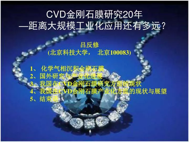
CVD 金刚石膜研究 20 年 — 距离大规模工业化应用还有多远?. 吕反修 ( 北京科技大学, 北京 100083). 1 、 化学气相沉积金刚石膜 2 、国外研究与产业化进展 3 、我国在 CVD 金刚石膜研究方面的现状 4 、我国在 CVD 金刚石膜产业化方面的现状与展望 5 、结束语. 与 CVD 金刚石膜有关的重大科技活动. 国际金刚石膜及相关材料应用会议 (ADC) - 两年一次 国际新金刚石科学与技术会议 (ICNDST) - 两年一次 欧洲金刚石膜及相关材料材料会议 - 每年一次 国际碳前沿技术会议 (FCT) - 两年一次.

E N D
CVD金刚石膜研究20年 —距离大规模工业化应用还有多远? 吕反修 (北京科技大学, 北京100083) 1、 化学气相沉积金刚石膜 2、国外研究与产业化进展 3、我国在CVD金刚石膜研究方面的现状 4、我国在CVD金刚石膜产业化方面的现状与展望 5、结束语
与CVD金刚石膜有关的重大科技活动 国际金刚石膜及相关材料应用会议(ADC) - 两年一次 国际新金刚石科学与技术会议(ICNDST) - 两年一次 欧洲金刚石膜及相关材料材料会议 - 每年一次 国际碳前沿技术会议(FCT) - 两年一次 NDNC 美国“星球大战”计划 欧洲“尤里卡”计划 中国“863”计划 日本先进碳前沿技术计划 Diamond and Related Materials Diamond Film Deposition - Science and Technology Diamond Films and Technology
CVD金刚石膜 硬度和 摩擦磨损特性 化学稳定性 摩擦磨损特性 光学性能 高热导率 半导体性质 声学性质 高功率、高 频率、抗辐 射电子器件 切削工具 光学窗口 超硬涂层 高保真扬 声器振膜 热沉 拉丝模芯 光学涂层 摩擦磨损 MCMs 高性能探测 器和传感器 高性能声 表面波器件 磨具磨料 X-射线窗口 高性能平板 显示和真空 微电子器件 半导体封装 电子对抗 捷变频雷达 X-射线光 刻掩膜 电化学应用
1980 1990 CVD Diamond DLC b-C3N4, CNx CVD Diamond DLC C-BN CVD Diamond DLC 2000 2005 CVD Diamond Nano Carbon Tube Nano diamond film CVD Diamond Nano Carbon Nano and Ultranano diamond Single crystal diamond Graphene !!!
AsTeX’s 75kW MWCVD System Norton’s High power dc arc plasma jet
CVD金刚石膜市场应用情况 市场应用 已有产品 重大工程 正在研发 • 金刚石薄膜 • 涂层工具 • 金刚石自支 • 撑膜工具 • 摩擦磨损 • 金刚石热沉 • SAW • SOD • 扬声器 • CVD单晶 • 光学材料和 • 另部件 • CO2激光窗 • 口 • 探测器和传 • 感器 • Ti-BDD电极 • 欧洲核聚变 • 中心微波窗 • 口 • ITER • 欧洲强子对 • 撞机 • 火星探测器 • 半导体光刻掩 • 膜 • 金刚石高温半 • 导体器件 • 探测器和传感 • 器 • MEMs • 生物医学应用 • 冷阴极器件
CVD金刚石膜新兴研究方向 • 纳米金刚石膜和超纳米金刚石膜 • 金刚石膜在MEMs和NEMs技术中的应用 • 大尺寸CVD金刚石单晶 • 金刚石膜电化学及生物医学应用
纳米金刚石膜和超纳米金刚石膜 纳米金刚石膜(NCD): 晶粒尺寸≦ 100nm 超纳米金刚石膜(UNCD): 晶粒尺寸仅为几个纳米 UNCD PCD NCD
纳米金刚石膜的制备 NCD UNCD 超高密度金刚石形核技术 超高速率金刚石二次形核技术 • 直流负偏压 • 金刚石粉研磨 • 高甲烷浓度形核 • 低温沉积 • C60沉积 • Ar-H2-CH4 • Ar-CH4
PCD NCD UNCD
纳米金刚石膜的特殊性质 • 具有和硼重掺杂金刚石膜一样的优异导电性能 • 比微米金刚石膜更加优异的场发射性能 • 极其光滑的表面, 无需抛光就可满足应用要求 • 极低的摩擦系数(0.07) ,比微米金刚石膜更低(0.1) • 具有超导特性
纳米金刚石膜的应用前景 • MEMs和NEMs元器件 • 金刚石膜基生物传感器和生物芯片件 • 光学涂层 • 高性能场发射平板显示器 • 真空微电子器件 • 摩擦磨损和工具涂层 有问题的应用 • 微电子器件的高导热封装
Ra 0.03mm Ra 0.42mm 纳米/微米金刚石膜复合涂层硬质合金工具切削性能比较
金刚石膜在MEMs和NEMs技术中的应用 • 极低的摩擦系数(0.01-0.1) • 最高的硬度 • 最高的弹性模量(刚度) • 极佳的化学惰性(常温下不与任何酸碱介质反应) • 高热导率 • 极佳的生物相容性 • 极佳的半导体性质
UV–visible absorption spectra of single-crystal CVD diamond (300 K). a) Before annealing, b) after annealed at 1800 °C for 2 min. The inset shows several examples of annealed diamond plates. Indentation patterns for as-grown (left), annealed near colorless (upper right), and ultratough single -crystal CVD diamond (lower right)
大尺寸CVD金刚石单晶应用前景 • 首饰 • 高性能金刚石辐射(粒子)探测器 • 高性能金刚石高温半导体器件 • 光学窗口 • 金刚石工具 • 高压物理研究(Anvil)
Diamond in Electrochemistry • Advantages of Diamond: • wide (>3.5 V)potential window • low background / noise • no electrode fouling/corrosion • low sticking coefficient • synthesis of fluorinated compounds • anodic destruction of organic wastes • reduction of metal ions (Li, Cd, Pb etc.) • nitrate and nitride reduction • electrochem. analysis • etc. G. Swain, A. Fujishima, V. Pleskov, M. Fryda, J. Foord, and others
Advantages for using diamond • Best bio-compatibility • Widest over-potential electrode • Best semiconductor • Excellent surface properties • Excellent optical properties
A conducting polymer layer on boron doped diamond (BDD) films used as the substrate for immobilization DNA molecules for hybridizing analysis Conductive polymer-modified boron-doped diamond for DNA hybridization Analysis, Huiru Gu, Xiaodi Su, Kian Ping Loh, Chemical Physics Letters388 (2004) 483–487
V G Reference electrode Epoxy Epoxy Epoxy Drain Drain Source Source Drain Drain Source Source Diamond Diamond Diamond Diamond Diamond based ISFET
Personal (home), clinical and hospital health care and Continuous monitoring of disease and treatment
金刚石膜产业化现状 • 工具与摩擦磨损应用 • 电子学应用 • 光学应用 • 热学应用 • 探测器与传感器 • 电化学应用 • 高保真扬声器金刚石振膜 • CVD金刚石单晶 • 其它
SemiCon SP3 Diamond film coated drills, endmills and inserts
Commercial CVD System for Diamond Cutting Tools CemeCon Company
热学应用 • 高功率激光二极管阵列热沉 • MCMs 金刚石基片 • 功率半导体器件金刚石封装 • LCD LD背光
问题?? • 性能价格比: • 金刚石膜与其它材料的连接 来自其它材料的竞争: SiC AlN Diamond/Cu composite
光学应用 • 高超音速导弹窗口和头罩 • 工业高功率CO2激光窗口 • 高功率微波窗口
Atlas Alice
国内研究和产业化进展情况 863计划 自然科学基金 创新基金 产业化
Present level of research for freestanding diamond films Tool Grade: Size:F120mm maximum Thickness: up to 2mm Fracture strength: 300MPa (as measured by three point bending method) Thermal grade: Thermal conductivity: from 8W/cm.k to 18W/cm.k Optical grade: Size: up to F60mm (F120mm possible by the end of June 2005) Thickness: up to 1.5mm Optical properties: Fully transparent from 0.22mm to mm wavelength microwave Mean transmitivity between 8 to 12 mm: ~70% ~87% (With oxidation resistant antireflection coatings) Thermal conductivity: 16W/cm.k (20W/cm.k maximum) Fracture strength: ≧ 300MPa Oxidation resistance: after exposure to laboratory air at 800℃ for 180s, the decrease in transmitivity in 8~12 mm wavelength range is less than 3% Resistant to 950℃ for 30s with a maximum transmission of 85% with coatings Dielectric loss at 5GHz: ~8x10⁻⁴ at 35GHz: ~3.6x10⁻⁴ Laser damage threshold: Pulsed YAG laser (1.06 mm, 10ns): 6~7 J/cm2 (6~7 x10⁸ W/cm2) Continuous wave CO2 laser: 115~226 kW/cm2
目前已经上市的产品和生产单位 • CVD金刚石拉丝模模芯, 砂轮修正笔等: • 北京人工晶体所 河北省科学院 • 核工业部九院 北京科技大学 • 浙江大学 宁夏机械研究院 • 吉林大学 • CVD金刚石薄膜涂层工具 • 北京科技大学 • 上海交通大学 • 中国工程物理研究院(9院) • 胜利油田 普莱斯曼公司 (普莱斯曼北京研发中心) 全部都是摩擦磨损应用 !!
正在进行研发的产品和技术 • 大尺寸光学级金刚石膜IR窗口 • 高功率行波管关键散热元件与应用技术 • 高功率电子器件散热元件与应用技术 • 污水处理BDD电极材料及应用技术 • 大尺寸CVD金刚石单晶 • 金刚石薄膜涂层硬质合金工具工业化生产技术 • 摩擦磨损应用