Download
1 / 35
380 likes | 604 Views
Analog Interfacing. These lecture notes created by Dr. Alex Dean, NCSU. In These Notes. Analog to Digital Converters ADC architectures Sampling/Aliasing Quantization Inputs M30626 ADC Peripheral Digital to Analog Conversion. Why It’s Needed.

E N D
Analog Interfacing These lecture notes created by Dr. Alex Dean, NCSU
In These Notes . . . • Analog to Digital Converters • ADC architectures • Sampling/Aliasing • Quantization • Inputs • M30626 ADC Peripheral • Digital to Analog Conversion
Why It’s Needed • Embedded systems often need to measure values of physical parameters • These parameters are usually continuous (analog) and not in a digital form which computers (which operate on discrete data values) can process • Temperature • Thermometer (do you have a fever?) • Thermostat for building, fridge, freezer • Car engine controller • Chemical reaction monitor • Safety (e.g. microprocessor processor thermal management) • Light (or infrared or ultraviolet) intensity • Digital camera • IR remote control receiver • Tanning bed • UV monitor • Rotary position • Wind gauge • Knobs • Pressure • Blood pressure monitor • Altimeter • Car engine controller • Scuba dive computer • Tsunami detector • Acceleration • Air bag controller • Vehicle stability • Video game remote • Mechanical strain • Other • Touch screen controller • EKG, EEG • Breathalyzer
ADC Output Codes Voltages V_ref 111..111 111..110 111..101 111..100 V_sensor ADC_Code 000..001 Ground 000..000 The Big Picture V_ref • Sensor detects air pressure and generates a proportional output voltage V_sensor • ADC generates a proportional digital integer (code) based on V_sensor and V_ref • Code can convert that integer to a something more useful • first a float representing the voltage, • then another float representing pressure, • finally another float representing depth // Your software ADC_Code = ad0; V_sensor = ADC_code*V_ref/1023; Pressure_kPa = 250 * (V_sensor/V_supply+0.04); Depth_ft = 33 * (Pressure_kPa – Atmos_Press_kPa)/101.3; Analog to Digital Converter PressureSensor AirPressure ADC_Code V_sensor
Getting From Analog to Digital • A Comparator is a circuit which compares an analog input voltage with a reference voltage and determines which is larger, returning a 1-bit number • An Analog to Digital converter [AD or ADC] is a circuit which accepts an analog input signal (usually a voltage) and produces a corresponding multi-bit number at the output. Comparator A/D Converter Vref Vin0 0 1 0 1 0 Vin1 Vin Clock
Digital value time Waveform Sampling and Quantization • A waveform is sampled at a constant rate – every Dt • Each such sample represents the instantaneous amplitude at the instant of sampling • “At 37 ms, the input is 1.91341914513451451234311… V” • Sampling converts a continuous time signal to a discrete time signal • The sample can now be quantized (converted) into a digital value • Quantization represents a continuous (analog) value with the closest discrete (digital) value • “The sampled input voltage of 1.91341914513451451234311… V is best represented by the code 0x018, since it is in the range of 1.901 to 1.9980 V which corresponds to code 0x018.”
The ADC produces a given output code for all voltages within a specific range The ideal transfer function A/D converter is a stair-step function. Consider a 2-bit ADC 0 to 4 V input LSB = 4/22 = 1 V Red line Truncation Maximum error is -1 LSB or + 0 LSB Blue line Rounding Maximum error in conversion is usually 1/2 bit. Half as much error if we limit range to Vref(1-2N/2) “3.0 V” “2.0 V” “1.0 V” “0.0 V” Transfer Function 11 1 LSB 10 Output Code 01 00 1.0 V 4.0 V 3.0 V 2.0 V Input Voltage
Transfer Function Equation General Equation n = converted code Vin= sampled input voltage V+ref = upper end of input voltage range V-ref = lower end of input voltage range N = number of bits of resolution in ADC Simplification with V-ref = 0 V ( ) 2 N V = + in n 1 / 2 ê ú V ê ú ë û + ref 10 3 . 30 v 2 ( ) = + = n 1 / 2 676 ê ú - N V V 2 5 v ë û - in ref = + n 1 / 2 ê ú - V V ê ú ë û + - ref ref X = I floor function: nearest integer I such that I <= X û ë
A multi-level voltage divider is used to set voltage levels over the complete range of conversion. A comparator is used at each level to determine whether the voltage is lower or higher than the level. The series of comparator outputs are encoded to a binary number in digital logic (a priority encoder) Components used 2N resistors 2N-1 comparators Note This particular resistor divider generates voltages which are not offset by ½ bit, so maximum error is 1 bit We could change this offset voltage by using resistors of values R, 2R, 2R ... 2R, 3R (starting at bottom) 7/8 V 6/8 V 5/8 V 4/8 V 3/8 V 2/8 V 1/8 V A/D – Flash Conversion 1V Comparators R + 1 R - + 1 R - + 1 R - + R 3 Encoder 0 - + 0 R - + 0 R - + 0 R - V in
ADC - Dual Slope Integrating • Operation • Input signal is integrated for a fixed time • Input is switched to the negative reference and the negative reference is then integrated until the integrator output is zero • The time required to integrate the signal back to zero is used to compute the value of the signal • Accuracy dependent on Vref and timing • Characteristics • Noise tolerant (Integrates variations in the input signal during the T1 phase) • Typically slow conversion rates (Hz to few kHz) Slope proportional to input voltage
Successively approximate input voltage by using a binary search and a DAC SA Register holds current approximation of result Set all DAC input bits to 0 Start with DAC’s most significant bit Repeat Set next input bit for DAC to 1 Wait for DAC and comparator to stabilize If the DAC output (test voltage) is smaller than the input then set the current bit to 1, else clear the current bit to 0 T T 4 6 T 5 T 3 T 2 T 1 know 10011x, try 100111 know 1001xx, try 100110 know 100xxx, try 100100 know 10xxxx, try 101000 know 1xxxxx, try 110000 know 100110. Done. ADC - Successive Approximation Conversion 111111 Test voltage(DAC output) AnalogInput 100110 100100 Voltage 100000 know xxxxxx, try 100000 000000 Start of Conversion Time
A/D - Successive Approximation Converter Schematic Converter Schematic
ADC Performance Metrics • Linearity measures how well the transition voltages lie on a straight line. • Differential linearity measure the equality of the step size. • Conversion time:between start of conversion and generation of result • Conversion rate = inverse of conversion time
Sampling Problems • Nyquist criterion • Fsample >= 2 * Fmax frequency component • Frequency components above ½ Fsample are aliased, distort measured signal • Nyquist and the real world • This theorem assumes we have a perfect filter with “brick wall” roll-off • Real world filters have more gentle roll-off • Inexpensive filters are even worse (e.g. first order filter is 20 dB/decade, aka 6 dB/octave) • So we have to choose a sampling frequency high enough that our filter attenuates aliasing components adequately
Quantization • Quantization: converting an analog value (infinite resolution or range) to a digital value of N bits(finite resolution, 2N levels can be represented) • Quantization error • Due to limited resolution of digital representation • <= 1/(2*2N) • Acoustic impact can be minimized by dithering (adding noise to input signal) • 16 bits…. too much for a generic microcontroller application? • Consider a 0-5V analog signal to be quantized • The LSB represents a change of 76 microvolts • Unless you’re very careful with your circuit design, you can expect noise of of at least tens of millivolts to be added in • 10 mV noise = 131 quantization levels. So log2 131 = 7.03 bits of 16 are useless!
Inputs • Multiplexing • Typically share a single ADC among multiple inputs • Need to select an input, allow time to settle before sampling • Signal Conditioning • Amplify and filter input signal • Protect against out-of-range inputs with clamping diodes
Some A/D converters require the input analog signal to be held constant during conversion, (eg. successive approximation devices) In other cases, peak capture or sampling at a specific point in time necessitates a sampling device. This function is accomplished by a sample and hold device as shown to the right: These devices are incorporated into some A/D converters Sample and Hold Devices
M30626 ADC Peripheral • For details see M16C/62P Hardware Manual (A/D Converter) • 10 bit successive approximation converter (bits=1), can operate in 8 bit mode (bits=0). • Input voltage: 0 to VCC • Reference voltage applied to VREF pin • Can be disconnected with VCUT bit to save power • Input Multiplexer: 26 input channels • Select one of three groups using adgsel1:0 • P10: 0 0 • P0: 1 0 • P2: 1 1 • Select one of the eight input channels in a group with ch2:0 • Or select ANEX0 or ANEX1 with opa0=1 or opa1=1
ADC Conversion Speed • Rates • With S/H: 28 fAD cycles for 8 bits, 33 for 10 bits (smp = 1) • Without S/H: 49 fAD cycles for 8 bits, 59 for 10 bits (smp = 0) • ADC clock generation • Can select fAD = fAD, fAD/2, fAD/3, fAD/4, fAD/6, fAD/12 (use cks2-0) • fAD= 24 MHz (see next page) • Frequency restrictions • fAD <= 10 MHz • fAD >= 1 MHz (using S/H) • fAD >= 250 kHz (not using S/H) fAD
CPU Clock System 32.768 kHz crystal oscillator here 1024 Hz 24 or 12 MHz 3 MHz 0.75 MHz 24 MHz 12 MHz ceramic or crystal oscillator here PLL doubles frequency 24 MHz
Conversion Modes • For details see M16C/62P Hardware Manual (A/D Converter) • Common operation details • Code starts conversion(s) by setting adst = 1 • Conversion stops… • When complete (ADC sets adst=0 as indicator) – in one-shot or single sweep mode • Code can also stop (set adst = 0) – primarily for repeat modes • Result is in result register (16 bits) for that channel (AD0-AD7, 0x03c0-0x03cf) • Modes • One-shot conversion of a channel (0) • Generates interrupt if ADIC register’s interrupt level is > 0 • Repeated conversion of a channel (1) • No interrupt generated, can read result register instead • Single sweep mode (2) • Converts a set of channels once: Channels 0-1, 0-3, 0-5 or 0-7 • Repeat sweep mode 0 (3) • Converts a set of channels repeatedly: Channels 0-1, 0-3, 0-5 or 0-7 • Repeat sweep mode 1 (7) • Converts a set of channels repeatedly: Channels 0, 0-1, 0-2 or 0-3 • Control Registers • ADCON0 (0x03d6), ADCON2 (0x03d4), ADCON1 (0x03d7)
QSK62P Board Analog Inputs • P10_0 (AN0) – Potentiometer (R135) • P10_1 (AN1) – Thermistor (RT101) • A thermistor’s resistance dependson its temperature • A voltage divider with a thermistor produces a voltage (VTh) which varies with temperature • The thermistor circuit on the QSK produces thesevoltages based upon theinput temperature • P10_2 – P10_7 – Unused • Port P0 – Unused • Port P2 – Unused
Checklist for Using ADC • Configure • I/O pin • set to input • ADC • AD clock speed • resolution • mode • sample and hold • trigger mode • connect reference voltage • Interrupt, if used • Set ADIC to non-zero value • enable interrupts (FSET I) • Set interrupt vector in sect30.inc to ADC ISR • Use • Select channel if it has changed (or hasn’t been set yet) • ch2-0 bits in ADCON0 • select port group • Start conversion • (Wait until done) • polling • interrupt • Get data and use • read from correct AD result register
Demonstrations • Polled one-shot conversion mode • Repeatedly convert input voltage and display value • Configure ADC • Main loop • Start conversion of channel 0 • Wait until it’s done • Convert result to text and display on LCD • Interrupt-driven one-shot conversion to fill buffer • Convert input voltage until input buffer is full, then stop • Configure ADC and interrupt controller • Main code • Start conversion of channel 0 • Wait until all conversions are done • Stop
One Shot ADC Mode – Demonstration Code #include "qsk_bsp.h" #include "stdio.h" #include "string.h" #define INPUT (0) unsigned position_code; void main(void) { char buf[9]; mcu_init(); // Initialize MCU adc_init(); // ADC too InitDisplay(); // LCD too while (1) { adst = 1; while (adst) ; position_code = ad0 & 0x03ff; sprintf(buf, "%d", position_code); DisplayString(LCD_LINE1,“ "); DisplayString(LCD_LINE1, buf); // display position } } void adc_init(void) { pd10_0 = INPUT; // To use channel 0 on P10 group as input /* clock selection: 24 MHz system clock, 6 MHz phiAD -> divide by 4 cks bits are 0 0 0 */ // ADCON 0 ch0 = 0; // channel 0 ch1 = 0; ch2 = 0; md0 = 0; // one shot md1 = 0; cks0 = 0; // divide clock by 4 // ADCON 1 trg = 0; // SW trigger md2 = 0; // one shot bits = 1; // 10-bit conversion cks1 = 0; // divide clock by 4\ vcut = 1; // connect reference voltage // ADCON 2 smp = 1; // use sample and hold adgsel0 = 0; // select port P10 group adgsel1 = 0; cks2 = 0; // divide clock by 4 }
Repeated ADC • The microcontroller performs repeated A/D conversions, and can read data whenever needed adcon0 = 0x88; adcon1 = 0x28; adcon2 = 0X01; adst = 1; // Start a conversion here • Then in your procedure TempStore = ad0 & 0x03ff;
Using ADC Values • The ADC gives an integer representing the input voltage relative to the reference voltages • Several conversions may be needed • For many applications you will need to compute the approximate input voltage • Vin = … • For some sensor-based applications you will need to compute the physical parameter value based on that voltage (e.g. pressure) – this depends on the sensor’s transfer function • You will likely need to do additional computations based on this physical parameter (e.g. compute depth based on pressure) • Data type • It’s likely that doing these conversions with integer math will lead to excessive loss of precision, so use floating point math • This requires using the floating point library (math.h). • AFTER you have the application working, you can think about accelerating the program using fixed-point math (scaled integers). We cover this in ECE 561. • Sometimes you will want to output ASCII characters (to the LCD, for example). You will need to convert the floating point number to ASCII via successive division or by using sprintf.
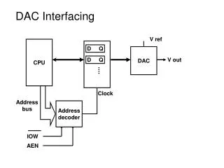
Vref Digital to Analog Conversion • May need to generate an analog voltage or current as an output signal • Audio, motor speed control, LED brightness, etc. • Digital to Analog Converter equation • n = input code • N = number of bits of resolution of converter • Vref= reference voltage • Vout= output voltage • Vout = Vref * n/(2N) D/A Converter 0 1 0 1 Vout
M30626 DACs • Two eight-bit DACs • DA0 is on port 9 bit 3 • DA1 is on port 9 bit 4 • Initialization • Configure port direction bit to input! This disables the digital logic output for that bit. • Enable DAC with enable bit DA0E or DA1E • Use • Write output values to data register DA0 or DA1
One Shot-Setting Control Interrupts adic = 0X01; /* 00000001; /* Enable the ADC interrupt ||||||||______interrupt priority select bit 0 |||||||_______interrupt priority select bit 1 ||||||________interrupt priority select bit 2 |||||_________interrupt request bit ||||__________reserved */ _asm (" fset i") ; // globally enable interrupts adst = 1; // Start a conversion here while (1){} // Program waits here forever } #pragma INTERRUPT ADCInt // compiler directive telling where // the ADC interrupt is located void ADCInt(void){ TempStore = ad0 & 0x03ff;// Mask off the upper 6 bits of // variable leaving only the result } // in the variable itself
Setting Control Registers & Interrupt To use interrupts, the ADC interrupt vector needs to point to the function. The interrupt vector table is near the end of the startup file “sect30.inc”. Insert the function label “_ADCInt” into the interrupt vector table at vector 14 as shown below. . . . .lword dummy_int ; DMA1(for user)(vector 12) .lword dummy_int ; Key input interrupt(for user)(vect 13) .glb _ADCInt .lword _ADCInt ; A-D(for user)(vector 14) .lword dummy_int ; uart2 transmit(for user)(vector 15) .lword dummy_int ; uart2 receive(for user)(vector 16) . . .. #pragma INTERRUPT ADCInt // compiler directive telling where // the ADC interrupt is located void ADCInt(void){ TempStore = ad0 & 0x03ff; // Mask off the upper 6 bits of // variable leaving only the result } // in the variable itself