Download
1 / 10
100 likes | 109 Views
Parallel Adaptive Equalizer Employing Sub-Convolution: VLSI Architecture Realized in a Field Programmable Gate Array. Andrew Gray, Scott Hoy. Jet Propulsion Laboratory California Institute Of Technology 4800 Oak Grove Drive M/S 238-343 Pasadena, CA 91109 September 9-11, 2003. Overview.

E N D
Parallel Adaptive Equalizer Employing Sub-Convolution: VLSI Architecture Realized in a Field Programmable Gate Array Andrew Gray, Scott Hoy Jet Propulsion Laboratory California Institute Of Technology 4800 Oak Grove Drive M/S 238-343 Pasadena, CA 91109 September 9-11, 2003
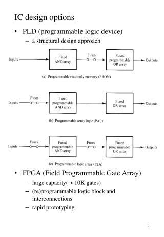
Overview • The paper provides an overview of a parallel adaptive equalizer architecture and its high-rate FPGA realization. • The all-digital equalizer targets high rate operation, hundreds of Mbps and higher. • The very large scale integration (VLSI) architecture for implementing a frequency domain least-mean squares (LMS) complex equalizer incorporates a simple sub-convolution method, digital vector processing, specialized FFT-IFFT hardware architectures, and the discrete Fourier transform-inverse discrete Fourier transform (DFT-IDFT) overlap and save filter method.
Fast Frequency Domain LMS • Block Length 8 • Overlap 50%, operating at 1/4th • 4 Coefficient Equalizer • 1/4th Rate Processing Architecture of Traditional Fast LMS For the conventional Fast LMS adaptive equalizer when the number of coefficients is increase, the FFT-IFFT lengths must also be increased.
Overlap-and-Save FIR Filter The Figure illustrates a parallel DFT-IDFT filtering architecture for frequency domain filtering or correlation using the overlap and save method. The DFT-IDFT length is L+1 (L is odd), and M, the downsample rate, is the number of samples the input window “slides”. The architecture has 50% input vector overlap, that is the downsample rate, is equal to half the input vector length, . With such a architecture a M+1 coefficient filter may be implemented in the frequency domain.
Sub-Convolution The convolution may be broken into numerous sub-convolutions, each time shifted input convolved with a sub-filter, as indicated.
Frequency Domain Fast LMS Employing Sub-Convolution and Sub-Correlation
Complexity Comparison • The figure is a plot of the approximate number of multipliers required to implement the three 16-coefficient equalizer architectures without hardware reuse. The fast LMS and block time-domain algorithms operate at 1/16th the input sample rate while the fast LMS using sub-convolution/correlation operates at 1/4th the input sample rate.
FPGA Implementation Xilinx Virtex 2 8-million gate FGPA device usage (xc2v8000-5-ff1152) Xilinx Virtex 2 8-million gate FGPA 12-coefficient parallel equalizer. Place and route timing constraints
Conclusion • The new architecture employs simple design techniques for designing parallel filter bank architectures based on the concept of separating a convolution and correlations into what we call sub-convolutions and sub-correlations. These techniques allow arbitrarily long convolution or correlation to be performed using the overlap-and-save method with virtually any FFT-IFFT length; the FFT-IFFT length may be chosen based solely upon the rate reduction desired. • The gate count and speed of the equalizer design implemented in the Xilinx FPGA was 1.142 million gates (uses 50% of slices and 85% of embedded 18x18 multipliers) running at a target clock speed of 55MHz. • The target speed of 75 MHz with 16-coefficients was desired but could not be attained in the high end Xilinx Virtex 2 (8 mega-gates) yet. • The non-fractionally spaced equalizer architecture presented operates at 1/4th the input symbol rate, uses 8-point FFT-IFFTs, has 12 coefficients and is extendable to higher tap lengths. Given the 55 MHz clock rate the equalizer can process and output in real time approximately 220 Mega-symbols per second; this results in processing data rates of 440 Mbps assuming QPSK type modulations and 880 Mbps assuming 16-QAM. Higher clock rates are possible with further “tweaking” of the design.