Download
1 / 46
480 likes | 597 Views
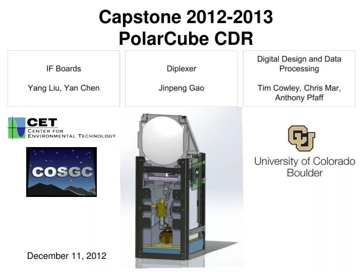
Capstone 2012-2013 PolarCube CDR. December 11, 2012. 2. Frequency vs. Zenith Opacity. Microwave Sounding. PolarCube will use 118.75 GHz, a resonance frequency of diatomic oxygen, as a center frequency. PolarCube Channels have a specified weights corresponding to altitude. 3.

E N D
Capstone 2012-2013 PolarCube CDR December 11, 2012
Frequency vs. Zenith Opacity Microwave Sounding • PolarCube will use 118.75 GHz, a resonance frequency of diatomic oxygen, as a center frequency • PolarCube Channels have a specified weights corresponding to altitude 3 Courtesy of Lavanya Periasamy, University of Colorado Courtesy of Dr. Gasiewski
Function of Radio Frequency (Channel 5) T=(F-1)T0 P=kTB
IF System 14
Diplexer Motivation • Multi-channel radiometer needs channel separation in order to measure different frequency band • The diplexer splits the signal from RF Receiver into two bands 15
Diplexer Design The design problem is much more difficult than it might at first seem. If ordinary low-pass filter and high-pass filter are simply connected together, interaction effects will usually disrupt the performance of the system, unless the filters and their interconnections are very carefully designed. To prevent this disruption, the complementary structure is very correct technique to design a diplexer. 16
Complementary Structure We construct diplexer with LPF and HPF to have complementary input admittances and connects them in parallel. The complementary input admittances means that the sum of the input admittance of the low pass and high pass filter are real and constant for all frequencies. Hypothetical input admittances of LPF and HPF is shown in the figure. 17
Idea Value VS. Real Value None of component manufacturer produces ideal component value. They produce limited discrete value and various size 19
Performances Ideal Value Real Value 21
Sum of Imaginary Part of Impedance Ideal Value Real Value -0.1 1.3 1.3 22
IF System • Two IF boards, in two carriers • The diplexer connected to the IF higher frequency circuit board(right hand box) 24 Courtesy of Space Grant Consortium, University of Colorado
IF System Risk Management • Physical constraint (shrink down the size of PCB boards) • Pre-amp signal oscillation problem (old design) • Fit in the video-amp board 26
Pre-Amp board and Oscillations 3-Amp Board Spectrum Analyzer Plot Have the peak in plot with 0 RF input signal 27
Video-Amp Layout Video Amp Board Signal Video Amp IF Board 29
Digital Hardware • Provides capability for communication over SPI with the ALL-STAR bus, for transmitting data and accepting/sending commands • Flash memory as needed for data queuing and workspace before transfer to ALL-STAR • Provides capability to sample the analog output of the IF system • Includes voltage regulators to provide necessary voltages to digital components 32
Software • Responsible for initiating and collecting samples from the output of the ADCs, communicating with ALL-STAR, and switching necessary components off during low-power availability • ALL-STAR server • Must compress data for transmission during downlink window • Manage power for components via control input to voltage regulators 33
SLOC 34
Digital Risk Management • Utilizing established Atmel SPI APIs to interact with digital hardware for quicker development • SVN SCM for distributed development and change tracking • Incremental hardware design strategy • Familiarization with software while hardware is being developed 35
Xplained Board • Risk mitigation strategy • Has allowed for familiarization with Atmel-provided SPI and GPIO APIs while test hardware is still being designed and ordered • Have used to verify the needed steps in getting one of the SPI interfaces to interact with Aardvark protocol analyzer • Familiarized with GPIO API for potential future use during power management 36
Modular Test Board Designs for Memory and ADCs Memory Test Board ADC Test Board 37
Power Constraints Power Supply Lines to Active Components in the Payload 39
Power Constraints and Preliminary Power Budget • Payload Power Supply: Nominally 4 - 5 W • Oscillator: 4.875W • Full Power Draw All Components: ~11W 40
Data Budget 42
Timeline 44
Acknowledgements Special Thanks to: Dr. Gasiewski Brian Sanders and the team at Space Grant Lavanya Periasamy Kyuil Hwang 45