Download
1 / 1
40 likes | 140 Views
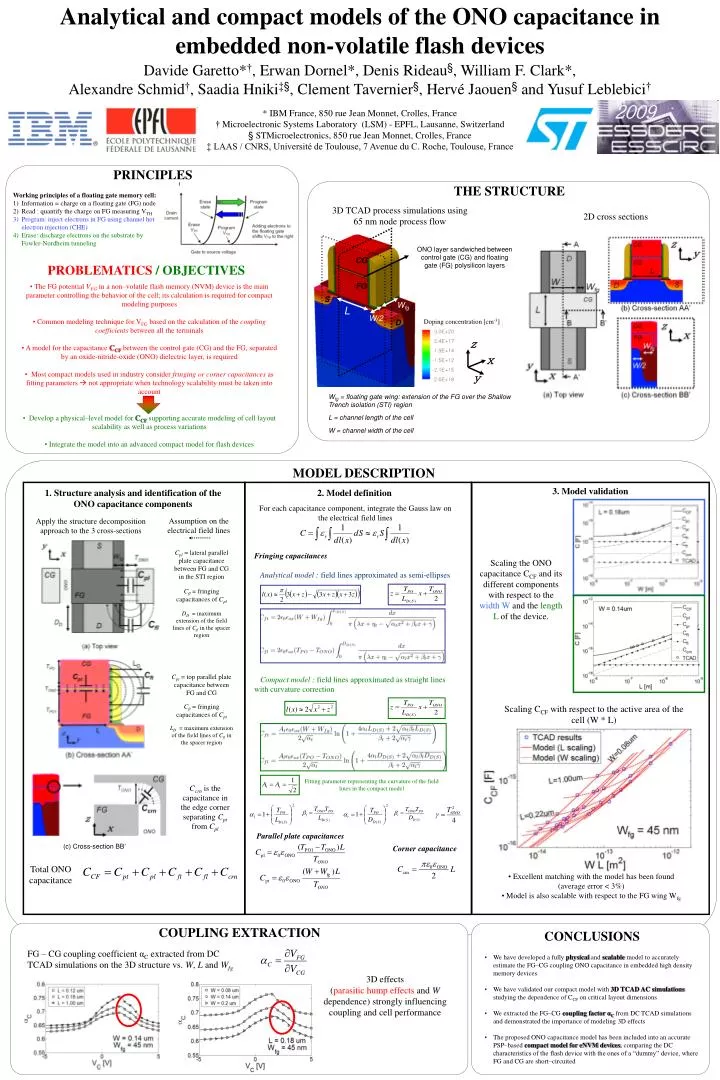
Analytical and compact models of the ONO capacitance in embedded non-volatile flash devices. 2D cross sections. (c) Cross-section BB’. Parallel plate capacitances. Corner capacitance. Davide Garetto* † , Erwan Dornel*, Denis Rideau § , William F. Clark*,

E N D
Analytical and compact models of the ONO capacitance in embedded non-volatile flash devices 2D cross sections (c) Cross-section BB’ Parallel plate capacitances Corner capacitance Davide Garetto*†, Erwan Dornel*, Denis Rideau§, William F. Clark*, Alexandre Schmid†, Saadia Hniki‡§, Clement Tavernier§, Hervé Jaouen§ and Yusuf Leblebici† * IBM France, 850 rue Jean Monnet, Crolles, France † Microelectronic Systems Laboratory (LSM) - EPFL, Lausanne, Switzerland § STMicroelectronics, 850 rue Jean Monnet, Crolles, France ‡ LAAS / CNRS, Université de Toulouse, 7 Avenue du C. Roche, Toulouse, France 2009 éé PRINCIPLES THE STRUCTURE • Working principles of a floating gate memory cell: • Information = charge on a floating gate (FG) node • Read : quantify the charge on FG measuring VTH • Program: inject electrons in FG using channel hot electron injection (CHE) • Erase: discharge electrons on the substrate by Fowler-Nordheim tunneling 3D TCAD process simulations using 65 nm node process flow ONO layer sandwiched between control gate (CG) and floating gate (FG) polysilicon layers CG PROBLEMATICS/ OBJECTIVES FG • The FG potential VFGin a non–volatile flash memory (NVM) device is the main parameter controlling the behavior of the cell; its calculation is required for compact modeling purposes • Common modeling technique for VFG based on the calculation of the coupling coefficients between all the terminals • A model for the capacitance CCF between the control gate (CG) and the FG, separated by an oxide-nitride-oxide (ONO) dielectric layer, is required • Most compact models used in industry consider fringing or corner capacitances as fitting parameters not appropriate when technology scalability must be taken into account • Develop a physical–level model for CCF supporting accurate modeling of cell layout scalability as well as process variations • Integrate the model into an advanced compact model for flash devices S Wfg L D W/2 Doping concentration [cm-3] D z x y Wfg = floating gate wing: extension of the FG over the Shallow Trench isolation (STI) region L = channel length of the cell W = channel width of the cell MODEL DESCRIPTION 3. Model validation 1. Structure analysis and identification of the ONO capacitance components 2. Model definition For each capacitance component, integrate the Gauss law on the electrical field lines Fringing capacitances Analytical model : field lines approximated as semi-ellipses Compact model : field lines approximated as straight lines with curvature correction Assumption on the electrical field lines Apply the structure decomposition approach to the 3 cross-sections Cpl = lateral parallel plate capacitance between FG and CG in the STI region Scaling the ONO capacitance CCF and its different components with respect to the width W and the length L of the device. Cfl = fringing capacitances of Cpl DD = maximum extension of the field lines of Cfl in the spacer region Cpt = top parallel plate capacitance between FG and CG Cft = fringing capacitances of Cpt Scaling CCF with respect to the active area of the cell (W * L) LD = maximum extension of the field lines of Cft in the spacer region Fitting parameter representing the curvature of the field lines in the compact model Ccrn is the capacitance in the edge corner separating Cpt from Cpl Total ONO capacitance • Excellent matching with the model has been found (average error < 3%) • Model is also scalable with respect to the FG wing Wfg COUPLING EXTRACTION CONCLUSIONS FG – CG coupling coefficient αC extracted from DC TCAD simulations on the 3D structure vs. W, L and Wfg • We have developed a fully physical and scalable model to accurately estimate the FG–CG coupling ONO capacitance in embedded high density memory devices • We have validated our compact model with 3D TCAD AC simulations studying the dependence of CCF on critical layout dimensions • We extracted the FG–CG coupling factor αC from DC TCAD simulations and demonstrated the importance of modeling 3D effects • The proposed ONO capacitance model has been included into an accurate PSP–based compact model for eNVM devices, comparing the DC characteristics of the flash device with the ones of a “dummy” device, where FG and CG are short–circuited 3D effects (parasitic hump effects and W dependence) strongly influencing coupling and cell performance