Download
1 / 1
10 likes | 123 Views
sp 2. sp 3. E LECTRON T RANSPORT IN M OLECULAR N ANOSTRUCTURES N anoscale S cience and E ngineering C enter, C OLUMBIA U NIVERSITY - G RANT N UMBER CHE-0641523 James T. Yardley, Managing Director; Tony Heinz and Ronald Breslow , Scientific Directors. NSEC. COLUMBIA UNIVERSITY

E N D
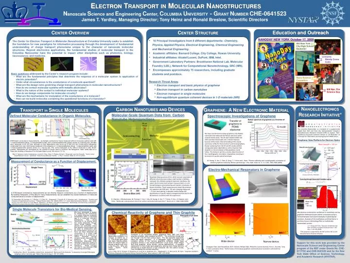
sp2 sp3 ELECTRON TRANSPORTIN MOLECULAR NANOSTRUCTURES NanoscaleScience and Engineering Center, COLUMBIAUNIVERSITY - GRANT NUMBER CHE-0641523 James T. Yardley, Managing Director; Tony Heinz and Ronald Breslow, Scientific Directors NSEC COLUMBIA UNIVERSITY IN THE CITY OF NEW YORK Education and Outreach CENTER STRUCTURE CENTER OVERVIEW Defined Molecular Conductance in Organic Molecules. NANODAY NEW YORK October 17, 2009 • 16 Principal Investigators from 6 different departments: Chemistry, Physics, Applied Physics, Electrical Engineering, Chemical Engineering and Mechanical Engineering. • Academic affiliates: Barnard College, City College, Rowan University. • Industrial affiliates: Alcatel/Lucent, DuPont, IBM, Intel. • Government Laboratory Partners: Brookhaven National Lab, Molecular Foundry (LBL), Network for Computational Nanotechnology, SRC (NRI). • Encompasses approximately 75 researchers, including graduate students and postdocs. • Research Thrust Areas: • Electron transport and basic physics of graphene • Electron transport in carbon nanotubes • Electron transport in single molecules • Non-equilibrium quantum coherent devices in 1-D materials (NRI) G mode The Center for Electron Transport in Molecular Nanostructure at Columbia University seeks to establish the foundation for new paradigms for information processing through the development of fundamental understanding of charge transport phenomena unique to the character of nanoscale molecular structures. Beyond electronics applications, the fundamental studies of molecular transport in the Columbia Nanocenter have the potential to impact other disciplines such as photonics, biology, neuroscience, and medicine. 400 New York City High School Students! Lectures: Wendy Crone Colin Nuckolls STM-based conductance measurements. (a) Sample conductance traces measured without molecules (yellow) and with 1,4-benzenediamine (blue), 1,4-benzenedithiol (red), and 1,4-benzenediisonitrile (green) shown on a semilog plot. (All data were measured at 25 mV bias, although no bias dependence was found up to 250 mV.) (b) Conductance histograms constructed from over 3000 traces measured in the presence of 1,4-benzenediamine (blue), 1,4-benzenedithiol (red), and 1,4-benzenediisonitrile (green) shown on a log-log plot. The control histogram of Au without molecules is also shown (yellow). Histograms are normalized by the number of traces used to construct the histograms. Inset: same data on a linear plot showing a Gaussian fit to the peak (black curve). Bin size is 10-4 G0. • Basic questions addressed by the Center’s research program include: • What are the fundamental principles that determine the response of a molecular system to application of electric potentials? • Under what circumstances is the conductance of a molecule quantized? • What are the design rules governing charge transport phenomena in molecular nanostructures? • How do we contact molecular systems with metallic electrodes? • What is the nature of the contact to individual molecular systems? • How do we design components for molecular circuitry? • What are the mechanisms for modulation of the conductance of a molecule? • How can we build molecules containing the operational functions of a transistor? Mark S. Hybertsen, Latha Venkataraman, Jennifer E. Klare, Adam C. Whalley, Michael L. Steigerwald, and Colin Nuckolls. “Amine-Linked Single-Molecule Circuits: Systematic Trends Across Molecular Families.” J. Phys.: Condens. Matter 20, 374115 (2008). Nano-Science Exposition Measurement of Conductance as a Function of Displacement. Bill Nye, The Science Guy. NANOELECTRONICS RESEARCH INITIATIVE* CARBON NANOTUBES AND DEVICES GRAPHENE: ANEW ELECTRONIC MATERIAL TRANSPORT in SINGLEMOLECULES In STM-based conductance measurements we can directly measure conductance as a function of displacement. By building histograms of this data for many measurements, we can establish the overall distribution of molecular conductances as a function of displacement. Current (nA) Molecular-Scale Quantum Dots from Carbon NanotubeHeterojunctions. Spectroscopic Investigations of Graphene Raman spectrum of graphene as a function of strain. M. Kamenetska, M. Koentopp, A. C. Whalley, Y. S. Park, M. L. Steigerwald, C. Nuckolls, M. S. Hybertsen, and L. Venkataraman. “Formation and Evolution of Single-Molecule Junctions.” Physical Review Letters 102, 126803 (2009); S. Y. Quek, Maria Kamenetska, Michael L. Steigerwald, Hyoung Joon Choi, Steven G. Louie, Mark S. Hybertsen, J. B. Neaton, and Latha Venkataraman. Mechanically controlled binary conductance switching of a single-molecule junction. Nature Nanotechnology 4, 234, 2009. Transfer of graphene to PDMS elastomer The Columbia Nanocenter is a recipient of a supplemental award from NSF and from the Semiconductor Industry’s Nanoelectronics Research Initiative (NRI) to explore “Non-equilibrium Quantum Coherent Devices in 1-D Materials” as a concept for information processing beyond CMOS silicon. We have transferred monolayer graphene onto flexible substrates and measured the Raman spectrum under uniaxial tensile strain. The 2D and G bands exhibit red shifts and the G band splits into 2 distinct features because of the strain-induced breaking of the crystal symmetry. Unlike for the G mode of unstrained graphene, Raman scattering from the G and G modes exhibits strong polarization dependence, with a response that depends on the orientation of the graphene crystal lattice. This behavior permits a precise determination of the crystallographic orientation of graphene monolayers by means of a purely optical technique. Graphene: New Platform for Electron Optics M. Huang, H. Yan, C. Chen, D. Song, T. F. Heinz and J. Hone. "Phonon softening and crystallographic orientation of strained graphene studied by Raman spectroscopy". Proc. Natl. Acad. Sci. U. S. A. 106, 7304-7308 (2009). Electro-Mechanical Resonators in Graphene Nanotubeheterojunctions (HJs), which connect nanotubes of different chiral structure using a small number of defects, represent the ultimate scaling of electronic interfaces. We report the first electrical transport measurements on a HJ formed between semiconducting and metallic nanotubes of known chiralities. These measurements reveal the presence of a quantum dot (QD) with ∼60 meV charging energy and ∼75 meV level spacing. A detailed model enables the identification of specific defect arrangements that lead to the QD behavior consistent with the experiment. SEM image of three graphene nanoribbons patterned by electron beam lithography and reactive ion etching. B. Chandra, J. Bhattacharjee, M. Purewal, Y. Son, Y. Wu, M. Huang, H. Yan, T. F. Heinz, P. Kim, J. B. Neaton and J. Hone. "Molecular-scale quantum dots from carbon nanotubeheterojunctions". NanoLett. 9, 1544-1548 (2009). Single Molecule Transistors for Bio-Medical Sensing. tunable mode (graphene) Chemical Reactivity of Graphene and Thin Graphite We observe conductance oscillations in extremely narrow graphene heterostructures where a resonant cavity is formed between two electrostatically created bipolar junctions. Analysis of the oscillations confirms that p–n junctions have a collimating effect on ballistically transmitted carriers We have developed a system for measuring the conductivity of a single molecule covalently immobilized within a nanotube gap in a molecular transistor architecture. This allows molecules to be directly wired into metal electrodes through robust amide linkages. The devices are sufficiently robust that aqueous environments can be used. In collaboration with the Jackie Barton group at Cal Tech, we have measured the conductivity of a single DNA duplex when it is wired into a carbon electrode through covalent bonds. Importantly, the presence of intervening mismatches attenuates DNA-mediated conduction leading to as much as 300-fold increase in resistance. These concepts can lead to new precision DNA sequencing technology. Histogram of pit sizes monolayer trilayer pits A. F. Young and P. Kim. "Quantum interference and Klein tunnelling in graphene heterojunctions". Nat. Phys. 5, 222-226 (2009). pits thick graphite bilayer *This program is supported by the NSF and the SRC via the Nanoelectronics Research Initiative. Exfoliated graphene flakes after oxidation in a furnace at 600°C for 2 hr. The single layer flake has been heavily pitted, while the bilayer flake is almost pristine with only a few tiny pits. Why are single layers more reactive? Surfaces of an exfoliated trilayer graphene flake (left) and thick graphite (middle), after oxidation at 600°C. The uniformly circular pits cut through only the first surface layer. The two samples apparently have the same reactivity. In a histogram (right) comparing the oxidation pitting of the various graphene surfaces, single layer graphene shows a very broad distribution of pit sizes, while trilayer and thick graphite show similar, narrow distributions. A possible explanation is that single layer graphene, lacking more freely deforms introducing a small amount of sp3 character into the carbon bonds, thus increasing the surface reactivity. Wide device Narrow device Support for this work was provided by the Nanoscale Science and Engineering Center program of the NSF under Grants No. CHE-0117752 and CHE-0641523 and by the New York State Office of Science, Technology, and Academic Research (NYSTAR). Changyao Chen, Sami Rosenblatt, Kirill I. Bolotin, William Kalb, Philip Kim, IoannisKymissis, Horst L. Stormer, Tony F. Heinz and James Hone. "Performance of monolayer graphene nanomechanical resonators with electrical readout“ In press. Li Liu, S. Ryu, M. R. Tomasik, E. Stolyarova, N. Jung, M. S. Hybertsen, M. L. Steigerwald, L. E. Brus and G. W. Flynn. "Graphene Oxidation: Thickness-Dependent Etching and Strong Chemical Doping". Nano Letters 8, 1965-1970 (2008). Xuefeng Guo, Alon A. Gorodetsky, James Hone, Jacqueline K. Barton and Colin Nuckolls. "Conductivity of a single DNA duplex bridging a carbon nanotube gap". Nature Nanotechnology 3, 163-167 (2008).