Download
1 / 15
150 likes | 250 Views
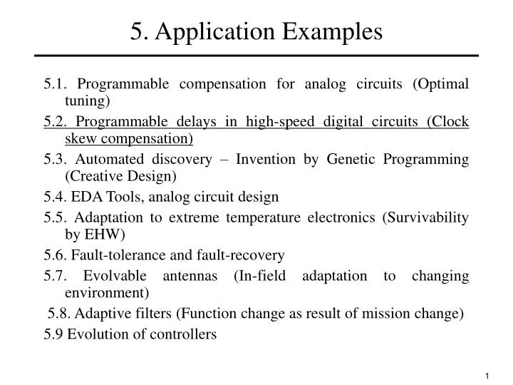
5. Application Examples. 5.1. Programmable compensation for analog circuits (Optimal tuning) 5.2. Programmable delays in high-speed digital circuits (Clock skew compensation) 5.3. Automated discovery – Invention by Genetic Programming (Creative Design) 5.4. EDA Tools, analog circuit design

E N D
5. Application Examples 5.1. Programmable compensation for analog circuits (Optimal tuning) 5.2. Programmable delays in high-speed digital circuits (Clock skew compensation) 5.3. Automated discovery – Invention by Genetic Programming (Creative Design) 5.4. EDA Tools, analog circuit design 5.5. Adaptation to extreme temperature electronics (Survivability by EHW) 5.6. Fault-tolerance and fault-recovery 5.7. Evolvable antennas (In-field adaptation to changing environment) 5.8. Adaptive filters (Function change as result of mission change) 5.9 Evolution of controllers 1
Post-Fabrication Clock Timing Adjustment • Design • Fabrication • Adjustment • Shipping LSI Design GA-based Adjustment Software • Low operating yield • Considerable power dissipation • Design clock speed + + • Higher operating yield • Less power dissipation • Faster clock speed than designed Programmable Delay Circuits LSI Tester EH-2003 talk: Power Dissipation Reductions with Genetic Algorithms Eiichi Takahashi Masahiro Murakawa, Yuji Kasai Tetsuya Higuchi. MIRAI Project /Advanced Semiconductor Research Center, AIST 2
Adaptive Clock Skew Compensation with GA Clock Lines Programmable Delay Element Problem: Tiny differences in propagation delay, when compounded across all the clock nets in a complex digital product, often lead to unacceptable degradations in overall system-timing margins. This generic problem is often referred to as the "clock skew" problem. Clock skew due to faster clock signals leads to degradation of operational yield rate of LSIs. Beyond 90nm, clock skew cannot be avoided only by design due to process variation Clock Input Programmable delay elements are inserted into clock inputs of FFs and circuit blocks. Delay values are determined optimally with GA EH-2003 talk: Power Dissipation Reductions with Genetic Algorithms Eiichi Takahashi Masahiro Murakawa, Yuji Kasai Tetsuya Higuchi. MIRAI Project /Advanced Semiconductor Research Center, AIST 3
Hierarchical Application of Clock Timing Adjustment Clock Domain or Circuit Block Clock Tree Circuit Sub-Block or Flip-Flop Clock adjustment required Clock adjustment not required Clock Driver Clock Domain, Circuit Block, or Flip-Flop Delay Circuit LSI Clock Input Clock not required Register (N bits) Clock Driver N Programmable Delay Circuit Clock Domain or Circuit Block LSI Clock adjustment for INTER-DOMAIN skew Clock adjustment for INTRA-DOMAIN skew EH-2003 talk: Power Dissipation Reductions with Genetic Algorithms Eiichi Takahashi Masahiro Murakawa, Yuji Kasai Tetsuya Higuchi. MIRAI Project /Advanced Semiconductor Research Center, AIST 4
Programmable Delay Circuit Delay Generator Delay Generator Clock In Clock Out DAC Vadj (Controlling Voltage) Register DAC (Digital-Analog Converter) Controlling Voltage (Vadj) vs Delay and Delay Steps P·A A P·A Delay [ns] Delay Step [ns] P·A A Delay Steps P·B P·A B Delay P·B P·B B P·C P·B C 30ps Vout (to Vadj) P·C P·C C Vref P·C Controlling Voltage [V] • 0.18um, CMOS process • 18Tr: Delay Generator + DAC • Some Delay Steps are less than 30ps “Delay Steps” are calculated as differences between adjacent delay plots. 5
Test Chip : Multiplier and Memory Test Pattern Generator Multiplier 0 p0 a0 0 0 p1 a1 0 0 p2 a2 0 0 p3 a3 0 b0 p4 Clock b1 p5 b2 Memory Test Pattern Generator p6 b3 p7 ALU Inverter Flip-flops X 9 Flip-flops X 9 Flip-flops X 5 Flip-flops X 4 Flip-flop + Decoder Programmable Delay Circuit = Ci Clock Input Full Adder Delay Setting Delay Setting Delay Setting Delay Setting = Programmable Delay Circuit Co 0.13um, CMOS process, Design for 1GHz(typ), Using the “Programmable Delay Circuits” EH-2003 talk: Power Dissipation Reductions with Genetic Algorithms Eiichi Takahashi Masahiro Murakawa, Yuji Kasai Tetsuya Higuchi. MIRAI Project /Advanced Semiconductor Research Center, AIST 6
Advantage No.1: Clock Frequency Speed-up LSI : Designed at 1000ps(=1GHz) period Register Register Register Register Circuit Data Input Data Output Circuit Circuit 800ps 1000ps 600ps Clock Input 1000ps(=1.0GHz) period 25% Enhancement of Clock Frequency (1000/800=1.25) LSI : Clock period is enhanced to 800ps(=1.25GHz) Register 0 Register Register Register Data Input Circuit Circuit Circuit 800ps 1000ps 600ps Clock Input 800ps(=1.25GHz) period 200ps-delay inserted EH-2003 talk: Power Dissipation Reductions with Genetic Algorithms Eiichi Takahashi Masahiro Murakawa, Yuji Kasai Tetsuya Higuchi. MIRAI Project /Advanced Semiconductor Research Center, AIST 7
Experiment Result:Clock Frequency Speed-up GHz Memory Test Pattern Generators Operational clock frequency BEFORE adjustment Operational clock frequency Operational clock frequency AFTER adjustment GHz Multipliers Each X point represents a unique chip • GA Details: • Population: 50 • Termination: 20th Generation • Selection: Tournament Selection • Crossover: One-Point Crossover • Crossover Rate: 1.0 • Mutation: Gaussian Mutation (σ=1.0) • Mutation Rate: 1.0 Operational clock frequency Each X point represents a unique chip 25% increase over all the chips EH-2003 talk: Power Dissipation Reductions with Genetic Algorithms Eiichi Takahashi Masahiro Murakawa, Yuji Kasai Tetsuya Higuchi. MIRAI Project /Advanced Semiconductor Research Center, AIST 8
Advantage No.2: Power Supply Voltage Reduction LSI which operates at standard power supply voltage 1.2V Register Register Register Register Register Data Input Circuit Circuit Circuit Circuit Data Output Circuit Circuit Circuit Circuit Clock Input Lowering power supply voltage, from 1.2V to 0.8V LSI which operates at lower power supply voltage 0.8V Register Register Register Register Register Data Input Circuit Circuit Circuit Circuit Data Output Circuit Circuit Circuit Circuit Clock Input Programmable Delay Circuit Circuits which violate timing constraints EH-2003 talk: Power Dissipation Reductions with Genetic Algorithms Eiichi Takahashi Masahiro Murakawa, Yuji Kasai Tetsuya Higuchi. MIRAI Project /Advanced Semiconductor Research Center, AIST 9
Experiment Result:Power Supply Voltage Reduction Operational yield at each voltage and clock frequency, BEFORE adjustment Voltage: 1.2V 1 2 0.8V Clock Adjustment & Operational yield at each voltage and clock frequency, AFTER adjustment Frequency: 1.0GHz 1.25GHz Measured with the Memory-test-pattern Generators. 3 EH-2003 talk: Power Dissipation Reductions with Genetic Algorithms Eiichi Takahashi Masahiro Murakawa, Yuji Kasai Tetsuya Higuchi. MIRAI Project /Advanced Semiconductor Research Center, AIST 10
Experiment Result:Power Dissipation Reduction 100% 3 1 Operational yield 0% 2 0.8V 1.2V Power Supply Voltage (Vdd) Reduction of 2/3 in Vdd: 1.2V 0.8V Power Reduction: 4/9 (-54%) Possible power reduction: 4/9 Reduction of 2/3 in Vdd Sakurai’s Formula for CMOS power dissipation [4]: where : Power supply voltage , : Almost constant : Clock frequency correspond to the same marks in Fig. 3 1 2 3 EH-2003 talk: Power Dissipation Reductions with Genetic Algorithms Eiichi Takahashi Masahiro Murakawa, Yuji Kasai Tetsuya Higuchi. MIRAI Project /Advanced Semiconductor Research Center, AIST 11
Time for Clock Timing Adjustment EH-2003 talk: Power Dissipation Reductions with Genetic Algorithms Eiichi Takahashi Masahiro Murakawa, Yuji Kasai Tetsuya Higuchi. MIRAI Project /Advanced Semiconductor Research Center, AIST 12
Experiment Result:Operational Yield Improvement Memory Test Pattern Generators Operating yield before adjustment 90.0% Yield improvement from 15% to 90% Operational yield [%] Operating yield after adjustment Multipliers 15.0% 93.3% Clock frequency [GHz] Operational yield [%] Yield improvement from 42% to 93% 41.6% While no chips were operational before adjustment, some chips were operational after post-fabrication adjustment. Clock frequency [GHz] EH-2003 talk: Power Dissipation Reductions with Genetic Algorithms Eiichi Takahashi Masahiro Murakawa, Yuji Kasai Tetsuya Higuchi. MIRAI Project /Advanced Semiconductor Research Center, AIST 13
Advantage No.3:Design Time Reduction Target Design: DDR-SDRAM controller circuit *1 *1 *1 day* person -21% EH-2003 talk: Power Dissipation Reductions with Genetic AlgorithmsEiichi Takahashi Masahiro Murakawa, Yuji Kasai Tetsuya Higuchi. MIRAI Project /Advanced Semiconductor Research Center, AIST 14
Summary of GA-based Post-Fabrication Adjustment Two 1GHz LSIs and a design experiment demonstrate advantages • Higher Clock Frequency (+25% max) • Smaller Area (saving circuits trying to avoid clock skew) • Reduced Design Time (-21% max) • Higher Yield • Lower Power Dissipation by lowering Power Supply Voltage (-54% max) EH-2003 talk: Power Dissipation Reductions with Genetic Algorithms Eiichi Takahashi Masahiro Murakawa, Yuji Kasai Tetsuya Higuchi. MIRAI Project /Advanced Semiconductor Research Center, AIST 15