Download
1 / 10
120 likes | 316 Views
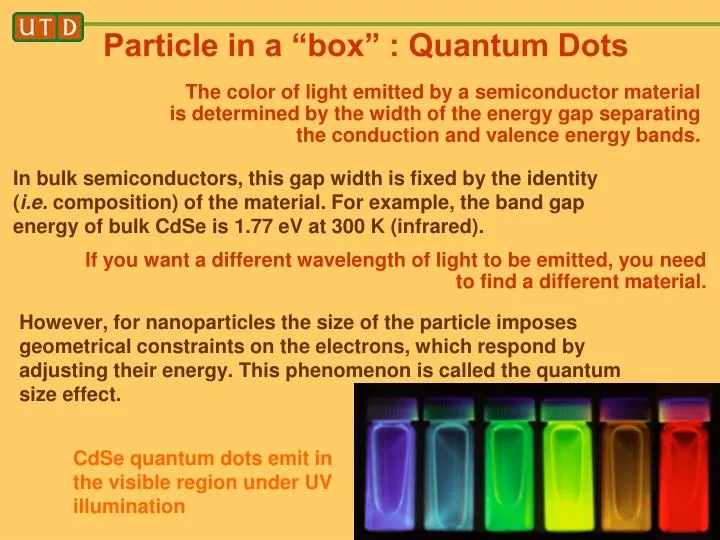
The color of light emitted by a semiconductor material is determined by the width of the energy gap separating the conduction and valence energy bands.

E N D
The color of light emitted by a semiconductor material is determined by the width of the energy gap separating the conduction and valence energy bands. In bulk semiconductors, this gap width is fixed by the identity (i.e. composition) of the material. For example, the band gap energy of bulk CdSe is 1.77 eV at 300 K (infrared). Particle in a “box” : Quantum Dots If you want a different wavelength of light to be emitted, you need to find a different material. However, for nanoparticles the size of the particle imposes geometrical constraints on the electrons, which respond by adjusting their energy. This phenomenon is called the quantum size effect. CdSe quantum dots emit in the visible region under UV illumination
Recall that a photon obeys for the relationship between the energy gap and the frequency or wavelength The quantum size effect can be approximately described by the “particle in a box” model. How good is this approximation?
CdSe quantum dots emit in the visible region under UV illumination
Scanning tunneling microscopy & spectroscopy (STM/ STS) Platinum-iridium tip [80/20, Pt does not oxidize (noble metal), Ir for strength] Substrate: gold-coated mica 50 to 250 mV potential difference (bias) Current flows due to applied bias Tunneling current: Positive bias: sample is positive, hence probe LUMO of sample Negative bias: sample is negative, hence probe HOMO of sample Particle in a box Particle in a box barrier
STM image of a monolayer of organic molecules In STM the bias is fixed and the tip is scanned across the sample. H.S. Lee, S. Iyengar, and I. H. Musselman, Anal. Chem. 2001, 73, 5532-5538
STM and STS of single wall carbon nanotubes In STS the tip position is fixed and the bias is scanned. The derivative of the current-voltage (I-V) curve gives the density of states and hence the bandgap for the semiconducting nanotube Ohmic vs. rectifying behavior: metallic vs. semiconducting nanotube