Download
1 / 26
290 likes | 461 Views
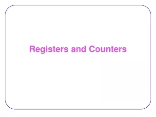
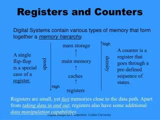
mass storage. main memory. density. speed. caches. registers. Registers and Counters. Digital Systems contain various types of memory that form together a memory hierarchy. high. A counter is a register that goes through a pre-defined sequence of states. A single flip-flop

E N D
mass storage main memory density speed caches registers Registers and Counters Digital Systems contain various types of memory that form together a memory hierarchy. high A counter is a register that goes through a pre-defined sequence of states. A single flip-flop is a special case of a register. high Registers are small, yet fast memories close to the data path. Apart from taking data in and out, registers also have some additional data manipulation capabilities. Digital Design Ed F. Deprettere Leiden University
REG Clear Clear = 0 all Q = 0 D0 D1 D2 D3 Q0 Q1 Q2 Q3 Clock from 0 to 1 Q(t+1) = D(t) A simple register 4 D-type flip-flops: positive edge triggered with negative logic asynchronous reset or clear input. Reading in data into the register is called loadingthe register. The loading is done in parallel if the four data bits are loaded simultaneously with a common clock. symbol Digital Design Ed F. Deprettere Leiden University
Loading on each clock pulse is (often) undesirable More control needed: Clock Load C inputs Register With Load Control C follows clock if Load is high ? clock skew ? • This is called clock gating. Take care! • What happens when 'Load' changes when the clock is low Clock and Gated Clock are not perfectly synchronized: a flip-flop using Clock and a flip-flop using Gated Clock don’t get activated at the same time. Digital Design Ed F. Deprettere Leiden University
Gating clock leads to clock skew: there is a propagationtime between the main clock and the C-inputs of various flip-flops, which are supposed to sense the same unique clock(t) in a clocked synchronous sequential circuit. Need some other mechanism: REG D = Load +DataIn Clear D0 D1 D2 D3 EN Q0 Q1 Q2 Q3 Better Register With Load Control • When Load = 0, FF content copied to itself (to get ‘no-change’!) • Build registers from these • General principle: don't gate the clock! Four times this structure to build 4-bit register with parallel load Digital Design Ed F. Deprettere Leiden University
Move bits laterally , west-to-east, east-to-west, north-to-south, south-to-north, or a combination of these, unidirectional or bi-directional. Principle: chain flip-flops: Serial Input Serial output SI D D D D SO C C C C Clock Clock SRG 4 SI SO The Shift Register Circuit Symbol Digital Design Ed F. Deprettere Leiden University
S A Cout B FA FA FA FA Cin S3 S2 S1 S0 example: the serial adder Recall: Parallel Adder is not really parallel! Carry ripples through roughly 2n gates: long propagation time. We can do better! Or, we can reuse a single FA: Serial Adder Idea: Use shift registers to store intermediate results. How? Digital Design Ed F. Deprettere Leiden University
Register A C SRG 4 FA Reset Clear X SI SO S Y C Shift Z Register B Clock SRG 4 C Clear Reset D SI SO Serial In C R Reset Ignoring Registers: Parallel adder is CC Serial adder is SC Serial addition is also called Software Addition. What about Power Dissipation? We say that the parallel adder has its states in space, the serial adder has its states in time. A typical example of space-time trade-off. More hardware faster. Less hardware slower. Digital Design Ed F. Deprettere Leiden University
Serial Input From Bus Serial output SI D D D D SO C C C C SI Shift Load Clock Data in Clock D Function Table SHR 4 C Shift Load Shift 0 0 no change 0 1 parallel load 1 X shift down Load Serial ! SI D0 D1 D2 D3 Q0 Q1 Q2 Q3 To Bus Serie-Parallel and Parallel-Serie Serial In, Parallel Out. Parallel In, Serial Out. Digital Design Ed F. Deprettere Leiden University
SHR 4 S1 S0 LSI D0 D1 D2 D3 RSI Q0 Q1 Q2 Q3 D Qi-1 Control Flip-flop Register Mode Operation C L(R)SI Left(Right) Serial In S1 S0 D S MUX 1 0 0 Qi No Change 0 1 Qi-1 Shift Down 1 0 Qi+1 Shift Up 1 1 Di Par. Load S 0 D Qi C 0 1 Di 2 3 D Qi+1 C Clock Bi-directional Shift Register Here is an up-down (bi-directional) shift register. Function Table If Qi = Q0, then Qi-1 = SI Digital Design Ed F. Deprettere Leiden University
Very useful device Produce time delay Example: 1 second-clock, count to 60 1 minute delay Control computation Example: serial adder, add 16 bits count to 16 Types of counters Asynchronous (ripple counter) — simple, but troublesome Synchronous counters (best kind) Up, down, special counters Counters with different periods Counters Digital Design Ed F. Deprettere Leiden University
Upward Counter Downward counter Gray code counter Q3 Q2 Q1 Q0 Q3 Q2 Q1 Q0 Q3 Q2 Q1 Q0 0 0 0 1 1 1 1 0 0 0 0 0 0 0 0 1 1 1 1 0 0 0 0 1 0 0 1 0 1 1 0 1 0 0 1 1 0 0 1 1 1 1 0 0 0 0 1 0 0 1 0 0 1 0 1 1 0 1 1 0 0 1 0 1 1 0 1 0 0 1 1 1 0 1 1 0 1 0 0 1 0 1 0 1 0 1 1 1 1 0 0 0 0 1 0 0 1 0 0 0 0 1 1 1 1 1 0 0 1 0 0 1 0 1 1 0 1 1 0 1 1 0 1 0 0 1 0 1 1 1 1 1 1 0 1 1 0 1 0 0 1 1 1 0 1 1 0 0 0 0 1 1 1 0 1 0 1 1 0 1 0 0 1 0 1 0 1 1 1 1 1 0 0 0 0 1 1 0 0 1 1 1 1 1 0 0 0 0 1 0 0 0 Counting Sequences Counters go through prescribed sequence of states upon application of input pulses (clock or other signals). Binary counter Binary counter Digital Design Ed F. Deprettere Leiden University
Clock D D D D C C C C • • R R • R R Q Q Q Q 1 3 2 0 Ripple Counter with T Flip-Flops Recall: T flip-flop Have seen this before. Remember? Features: Simple Clock input from logic circuits — not quite clock synchronous Digital Design Ed F. Deprettere Leiden University
enable D Q C CTR 4 C Q0 EN Q1 Q2 Q3 CO Carry out clock Synchronous Counters Clock goes to all flip-flops. Digital Design Ed F. Deprettere Leiden University
CTR 4 CTR 4 Load Count D0 D1 D2 D3 Load Count D0 D1 D2 D3 Q0 Q1 Q2 Q3 C0 1 Q0 Q1 Q2 Q3 C0 0 Many more counters can be thought of. Up-down counters: can go both ways for k = 0 step +1 to 7, or for k = 7 step –1 to 0 increment decrement Counters with parallel load: can be initialized N = 1; for k = N step +1 to N+7 parametrized Symbol Example: BCD counter. Digital Design Ed F. Deprettere Leiden University
Count sequence Present State Next State A B C A B C 0 0 0 0 0 1 0 0 1 0 1 0 0 1 0 1 0 0 1 0 0 1 0 1 1 0 1 1 1 0 1 1 0 0 0 0 0 1 1 → 1 1 0 1 1 1 → 0 1 0 Designing Counters Input Equations: D(A) = A B (m3 is x) D(B) = C D(C) = B C Digital Design Ed F. Deprettere Leiden University
control Data out Control unit Datapath Control in status Control out Data in Register Transfer Basic Digital Systems consist of • a datapath → performs operations on data • a control unit → determines the sequence of operations • one or more levels of memory → caches Datapaths consists of • registers → small and fast memories (basic components) • operations performed on data in registers (load, clear, shift, count) Registers → elementary operation → registers: register transfer operations Elementary operations: microoperations. Digital Design Ed F. Deprettere Leiden University
16 15 14 13 12 11 10 9 8 7 6 5 4 3 2 1 0 DA AA BA M FS M W B D R Control word n Register file: m m is number of address bits: 2 registers Write D data D address A address B address A data B data m m n 2 Register file m m Constant in 1 0 Mux B MB select Address out n n Data out Bus A Bus B 5 A B Function unit FS V C N Z Data in F MD select 0 1 Mux D Datapath three registers can be active at the same time: 2 (A,B) to read from, 1 (D) to write to all in one clock cycle. Buses: 2 buses, bus A and bus B, n-bit wide. Mux B selects between RF and Constant. Function unit: Contains arithmetic/logic unit (ALU) and Barrel shifter. FS is a function select code. Status bits are Z (1 if result is all 0), N (sign) C (carry) and V (overflow). Digital Design Ed F. Deprettere Leiden University
15 0 15 8 7 0 R1 PC(L) PC(H) t : B goes high t+1: transfer occurs B B: R1(7:0) R2(7:0), R2(7:0) R1(7:0), R3 M[R4] B Load R2 R1 n Boolean condition Transfer if B = 1 Simultaneously Memory to register Memory address in R4 Other example: ( if-then-else) B1: R0 R1, B1B2: R0 R2 Registers R and PC are names of registers. (or PC(15:8) and PC(7:0) Transfer operations: Digital Design Ed F. Deprettere Leiden University
n load enable n Write D data D address A address B address A data B data m 2 Mux B m decoder n 2 Register file R0 m m decoder Mux A 2 2 Load R Load Enable Bus n R0 R2 R1 n R0 R1 R2 R1 Bus MUX Select Load Enable Register File & Bus Register transfer here is multiplexer based. Bus based is another possibility: Digital Design Ed F. Deprettere Leiden University
Address Decoder Data bus destination decoder Timing/control Enable Data bus source decoder R1 A0 A1 A2 Enable Load R1 D0 D1 D2 Address bus k Data bus n Read Write k 2 n memory Read: Dx M[Ax] Write: M[Ax] Dx Examble: Memory transfer Digital Design Ed F. Deprettere Leiden University
5 A B Function unit FS V C N Z H select G select 5 B A B ALU Shifter F S S2:0 || Cin 4 2 0 0 IR IL H G Zero Detect A n-bit G MF select Mux F B parallel adder S0 S1 Cout Cin F : A, A, B, A+1, A-1, A+B A+B, A+B+1, A+B+1. MF=0, S2=0,Arithm. MF=0, S2=1, Logic 0 = ALU 1 = Shifter Gselect MF=1 Hselect Function unit Consists of an ALU and a Shifter. Suppose ALU is: Micro operations: F FS = MFselect S2 S1 S0 Cin F : AB, AB, AB. F : srB, slB Digital Design Ed F. Deprettere Leiden University
With Shifter words can be shifted right or left , over one or more bits: . Alternative: combinational circuit: . B0 IR IL 0 1 2 m u x 0 1 2 m u x 0 1 2 m u x 0 1 2 m u x S S S S 2 H0 Barrel Shifter is similar (bit more involved) but allows to shift over more than one bit (2 m >0 or m<0) m Moving in a 0 at the most or least significant bit position or rotated: Entering outgoing bits at the other side (wrap around) The bidirectional shiftregister with parallel load could be used. Cost: three clock pulses (load into SR, shift, transfer to R) Digital Design Ed F. Deprettere Leiden University
RTL symbolics Meaning R0 R1 + R2 contents of R1 plus R2 transferred to R0 R2 R2 1’s complement of content of R2 R2 R2 + 1 2’s complement of content of R2 R0 R1 + R2 + 1 contents of R1 minus R2 transferred to R0 R1 R1 + 1 increment content of R1 R1 R1 – 1 decrement content of R1 R2 XB: R1 R1 + R2, XB: R1 R1 + R2 + 1 Cn-1 Adder/subtractor X (B1 + B2) : R1 R2 + R3, R4 R5 R6 Cn B R0 R1 logic NOT R0 R1 R2 logic AND R0 R1 R2 logic OR R0 R1 R2 logic XOR V C R1 R1 sl R2 shift left R1 sr R2 shift richt Micro operations Arithmetic, logic and shift micro operations. Logic plus (OR) Microoperation OR Meaning: 1’s complement, clear bits, set bits, complement bits Digital Design Ed F. Deprettere Leiden University
15 14 13 12 11 10 9 8 7 6 5 4 3 2 1 0 • DA AA BA M FS M R • B D W • R1 R2 R3 R A + B + 1 F W • 001 010 011 0 00101 0 1 Bit Field Symbolic Binary Microoperation: R1 R2 + R3 +1 Control Word encoding. Timing (simulation). Depends on the complexity of the combinational circuit parts. Assume: propagation delays of CC parts are small with respect to clock period. This means that status bits, Address out and Data out (MB = 0) change at the same time as the register values. Changes in registers as a result of a microoperation appear at the clock cycle after that in which the microoperation is specified. (positve edge triggered FFs!) Values of status bits, Address out and Data out appear in the same clock cycle. Values of Constant in and Data in are placed in the clock cycle in which they are Needed. Digital Design Ed F. Deprettere Leiden University
n 3ns 3ns 1ns 4ns 1ns Write D data D address A address B address A data B data Clock m m n 2 Operand fetch 4ns Execute 4ns Write back 4ns Total 12ns Register file m m Constant in 1 0 MB select Mux B 1ns Address out n n Bus A Bus B Data out 5 A B Function unit FS Operand fetch 4ns Execute 5ns Write back 5ns Total (say) 15ns V C N Z Data in 1ns F MD select 0 1 Mux D Pipelined Datapath Suppose datapath design leads to a maximum clock frequency of 83.3 Mhz, because: All to be done in one clock cycle of 12ns. Introduce two extra registers (pipeline registers) i.e,2 extra ns. All to be done in one clock cycle of 15ns? NO! Digital Design Ed F. Deprettere Leiden University
OF OF OF OF OF OF EX EX EX EX EX EX WB WB WB WB WB WB Microinstruction k k+1 k+2 Pipeline is filling fully utilized emptying No, Because, due to pipeline registers, we can do Write back of microinstruction k (5ns) Execute of microinstruction k + 1 (5ns) Fetch operand of microinstruction k + 2 (5ns) In the same clock period of 5 ns, which is at 200Mhz clock frequency Clock period 1 2 3 4 (k) 5 (k+1) 6 (k+2) 78 Is 2.4 times as Or: throughput (# Ops/cc) many Ops. is 2.4 as high. In ideal case(neglecting filling/emtying):one microinstruction/clock cycle, of 5ns, as compared to one microinstruction/clock cycle of 12ns. Digital Design Ed F. Deprettere Leiden University