Download
1 / 48
490 likes | 814 Views
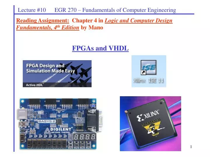
Lecture #10 EGR 270 – Fundamentals of Computer Engineering. Reading Assignment: Chapter 4 in Logic and Computer Design Fundamentals, 4 th Edition by Mano. FPGAs and VHDL. Lecture #10 EGR 270 – Fundamentals of Computer Engineering. Programmable Devices

E N D
Lecture #10 EGR 270 – Fundamentals of Computer Engineering Reading Assignment: Chapter 4 in Logic and Computer Design Fundamentals, 4th Edition by Mano FPGAs and VHDL
Lecture #10 EGR 270 – Fundamentals of Computer Engineering • Programmable Devices • There are three types of programmable devices: • Programmable Logic Devices (PLDs) • Contain many macrocells, consisting of large arrays of AND/OR gates and flip-flops. • PLA or PAL architecture limits their use for complex functions. • Simple architecture works well for consisting delay paths. • Complex Programmable Logic Devices (CPLDs) • Multiple PLD blocks with programmable interconnections. • Improvement over PLD, but architecture is still limited. • Simple architecture works well for consisting delay paths. • Field Programmable Gate Arrays (FPGAs) • Based on large numbers of Configurable Logic Blocks (CLBs) with a network of interconnects allowing for complex functions. • Very flexible architecture. • Designs can emphasize minimum delay or minimum area. • FPGAs may also include areas RAM, dedicated paths for fast arithmetic operations, embedded processors, and more.
Lecture #10 EGR 270 – Fundamentals of Computer Engineering • Xilinx CoolRunner-II CPLD Family • Features • - Densities from 32 to 512 macrocells • Function block feature PLAs with up to 56 product terms • 6000 gates for 256 macrocell version • Xilinx Spartan-3E FPGA • Features • - 100k to 1.6M gates • 66 to 376 I/Os • up to 36 18x18 multipliers • up to 648kbits of block RAM
Lecture #10 EGR 270 – Fundamentals of Computer Engineering • Field Programmable Gate Arrays (FPGAs) • The FPGA consists primarily of: • Configurable Logic Blocks (CLBs) • Input/Output Blocks (IOBs) • RAM Blocks • Programmable Interconnects between the CLBs
Lecture #10 EGR 270 – Fundamentals of Computer Engineering Configurable Logic Blocks (CLBs) and Programmable Interconnects The CLBs can be interconnected through programmed connections.
Lecture #10 EGR 270 – Fundamentals of Computer Engineering • CLB structure • CLBs are divided into “slices” and each slice contains two sets of the following: • Look Up Table (LUT) • Essentially a 16x1 RAM • Can be used to implement any 4-input logic functions • Can be configured as a 16-bit shift register • Carry and Control Logic • Arithmetic logic, multiplexer logic, multiplier logic • Can be used to bypass register for combinational outputs • Register (D flip-flop) • For sequential logic The LUT is a key element in an FPGA. The Xilinx Spartan-3E FPGA used in lab has 1920 LUTs.
Lecture #10 EGR 270 – Fundamentals of Computer Engineering Look Up Tables (LUTs) The LUT is a key part of an FPGA. A 4-input LUT acts essentially like a 16 x 1 RAM and can be used to implement any logic function with up to 4 inputs and 1 output.
LUT LUT LUT LUT Lecture #10 EGR 270 – Fundamentals of Computer Engineering Look Up Tables (LUTs) LUTs can be cascaded together to form larger logic functions. Two LUTs are used below to implement a function with 5 inputs. OUT
Lecture #10 EGR 270 – Fundamentals of Computer Engineering • Other FPGA features • FPGAs also contain a number of other features including: • Dedicated paths to allow for fast carries in addition • Multipliers • Embedded microprocessors - System on a Chip (SoC) • Blocks of RAM (embedded memory) • Some newer FPGAs use 6-input LUTs • Another difference between PLDs and FPGAs • Note that PLDs are EEPROM based so that downloaded designs are not lost when the device is powered down. • On the other hand, most FPGAs are SRAM-based (LUTs are small SRAMs). Therefore if you download a design into an FPGA and then power down the device, the design is lost. However, FPGAs often include separate EEPROM which can be used to reload the design when the device is powered up. We will see this in lab.
Lecture #10 EGR 270 – Fundamentals of Computer Engineering FPGA applications - Automotive Under-the-Hood Electronics - Automotive Entertainment Systems- Cellphones & Communicators - Customer Premises Equipment- Wired Communications Infrastructure - Wireless Communications Infrastructure- Compute Platforms - HDDs & Storage Systems- Office Equipment & Computer Peripherals - Wired Games Consoles- Handheld Games Consoles - Media Players/MP3 Players- Cameras & Camcorders - TVs & Set-top Boxes- DVD Recorders & Players - Other Consumer Electronics- Industrial Automation & Drives - Medical Electronics- Chip Cards & Payment Processing - Other Industrial Electronics- Military/Aerospace http://www.researchandmarkets.com/reports/836306
FGPA Applications SMT387-VP20-6 Disk Storage Controller
FGPA Applications Data Acquisition and Playback board
Lecture #10 EGR 270 – Fundamentals of Computer Engineering FPGAs versus ASICs FPGAs are user-programmed devices and are often sufficient for small volume projects. As volume increases, designs can be sent to semiconductor manufacturers to fabricate custom devices, or Application Specific Integrated Circuits (ASICs). • ASICs • High performance • Low power • Lower cost for high volume (perhaps > 250,000 devices) • More efficient routing • Long lead time needed for time-consuming fabrication at manufacturing facility • Design changes very expensive • FPGAs • Use off-the-shelf devices • Short time to market • Easily modified • Low development cost • Cost effective for low volume (perhaps < 250,000 devices) • Routing limitations may limit size of design (perhaps only half of the available gates can be effectively used)
Lecture #10 EGR 270 – Fundamentals of Computer Engineering FPGAs versus ASICs Gartner: ASIC design starts to fall by 22% in '09Dylan McGrathEE Times (03/30/2009)SAN FRANCISCO—FPGAs are displacing ASICs—a trend that in 2009 will be exacerbated by the global financial crisis—and now have a 30-to-one edge in design starts, according to market research firm Gartner Inc. ASIC design starts are expected to drop by 22 percent in 2009 as the economy causes firms to push out and—in some cases—cancel designs, Gartner (Stamford, Conn.) said.
Lecture #10 EGR 270 – Fundamentals of Computer Engineering Major FPGA manufacturers SRAM-based FPGAs Xilinx, Inc. Altera Corp. Atmel Lattice Semiconductor Flash & antifuse FPGAs Actel Corp. Quick Logic Corp. Xilinx and Altera represent about 60% of the FPGA market • Notes: • Volatile memory, including SRAM and DRAM, loses its information when powered down. • Non-volatile memory, including flash memory, does not lose its power when powered down. • Most FPGAs are currently SRAM-based. They are easier to manufacture, as well as denser (40 nm versus 150 nm) and cheaper.
Lecture #10 EGR 270 – Fundamentals of Computer Engineering Xilinx FPGAs • Old families • XC3000, XC4000, XC5200 (old 0.5µm, 0.35µm and 0.25µm technology) • High-performance families • Virtex (0.22µm), Virtex-E, Virtex-EM (0.18µm) • Virtex-II, Virtex-II PRO (0.13µm) • Virtex-4 (90 nm) • Virtex-5 (65 nm) • Virtex-6 (40 nm) • EasyPath-6 (lower cost version based on Virtex-6 design) • Low Cost Family • Spartan/XL, Spartan-IIE • Spartan-3E (90 nm, 100k – 1.5M gates) • Note: We will use the Spartan-3E with 100k gates in lab • Extended Spartan 3A (90 nm, 50k – 3.4M gates) • Spartan-6 (45 nm) What’s next? Xilinx and Altera are working on 28 nm technology FPGAs
Lecture #10 EGR 270 – Fundamentals of Computer Engineering Spartan-3E FPGA Specifications Spartan-3E XC3S100E is used in lab Other Xilinx FPGAs
Lecture #10 EGR 270 – Fundamentals of Computer Engineering Spartan-3E FPGA Development Boards It is common to use development boards to test your designs. The board provides easy access to I/Os, ports (USB, video, etc). Once a design has been developed, the FPGA may be placed on a custom board within the desired commercial application. Spartan-3E Eval Board Digilent BASYS2 FPGA Board (100k or 250k) Digilent NEXYS2 FPGA Board (500k gates) Spartan-3E Starter Kit
Lecture #10 EGR 270 – Fundamentals of Computer Engineering • Digilent BASYS2 FPGA Board • Digilent is a company that makes FPGA boards for educational use. The BASYS2 board uses the Xilinx Spartan-3E FPGA and is available with either 100k gates ($59) or 250k gates ($79). Digilent also produces the NEXYS2 board which uses the Xilinx Spartan-3E FPGA with 500k gates ($99). • We will use the BASYS2 board in lab. Our BASYS2 features: • 100 k gates • 1920 LUTs (slices) • 8 slide switches for inputs • 4 pushbutton switches for inputs • 8 LEDs for outputs • Four 7-segment displays for outputs • USB2 port, VGA port, and PS2 port • Multiple clock sources (1 Hz, 25 MHz, 50 MHz, 100 MHz) • FPGA board can be powered through the USBs connection or separately • Four 6-pin Pmod (peripheral module) connectors for external circuitry and devices • Flash ROM to store programmed connections • 72k Block RAM, 15k Distributed RAM • 4 dedicated multipliers
Digilent BASYS2 FPGA Board 8 LEDs Jumper JP3 (PC or ROM mode) Four 6-pin Pmod connectors PS2 Port (keyboard) VGA Port (video) USB2 Four 7-segment displays Power Switch 8 slide switches 4 push-button switches
Digilent BASYS2 Board Pinout – The pinout shown includes pin numbers (G12, C11, etc) for the input switches and the output LEDs and 7-segment displays. LEDs: active-HIGH (light when output is HIGH) Button Switches: produce a HIGH input when pressed 7-segment Displays: common-anode displays, so a LOW on CA turns on segment a. Note that all like segments are tied together on the 4 displays. To turn on a display, it must be enabled (or “asserted”) using AN0 – AN3 (active-LOW). So if AN0 is LOW, then display 0 is enabled. If AN3 is HIGH, then display 3 is disabled. To use more than one display at a time, they must be multiplexed (the human eye can’t tell if each display is actually ON for only ¼ of the time if multiplexed at a 60 Hz rate).
Digilent BASYS2 FPGA Board • The Spartan-3E is available in different packages. The CP132 package is used on the BASYS2 board. In the CP132 package 132 pins are arranged in columns (1-14) and rows (A-P) as shown below. Legend
Digilent BASYS2 FPGA Board • Full pinout
How do we program an FPGA? - 3 steps: • HDL Programming Tool • FPGAs are programmed in VHDL or Verilog • Programs could be used with any FPGA • Dominant VHDL software: Aldec Active-HDL and ModelSim • Others: Xilinx ISE, Quartus II, BlueHDL, VHDL Simili, …. • Synthesis Tool • Used to implement or “synthesize” the VHDL design into a specific FPGA • Synopsis Synplify – works with various manufacturer’s FPGAs • Xilinx ISE for Xilinx FPGAs • Quartus II for Altera FPGAs • ispLever for Lattice FPGAs (or Synopsis Synplify Lattice Edition) • Downloader • Used to download the design into a specific FPGA board • Example: Digilent Adept is used for the Digilent BASYS2 FPGA Board
What specific software will we use in lab to program an FPGA? Aldec Active-HDL 8.1 Describe circuit design using VHDL vhd file (e.g., MyFile.vhd) • Xilinx ISE 11 • Synthesize design for Xilinx Spartan-3E FPGA bit file (e.g., MyFile.bit) Digilent Adept Download to specific FPGA board: Digilent BASYS2 with Spartan-3E USB2 cable Digilent BASYS2 FPGA Board
Lecture #10 EGR 270 – Fundamentals of Computer Engineering • Hardware Description Language (HDL) • Until the 1980’s schematics were the primary means for describing digital circuits and systems. Hardware description languages (HDLs) were introduced in the 1980 for specifying logic equations to be used in PLDs. • In the 1990’s the use of PLDs, CPLDs, and FPGAs grew as the devices became inexpensive and denser (containing a larger number of equivalent gates). • It has become increasingly difficult to describe large digital circuits and systems with schematics alone and now HDL’s have become the primary tool for digital designer to design large digital systems. HDL’s can be used to describe both top-level and detailed module-level digital systems. • Computer programmers typically use high-level languages like C++ or Java so that they can deal with larger, more complex programs compared working with detailed assembly language programs. In a similar manner, HDL’s allow digital designers to describe large, complex systems without working at the detailed schematic level.
Lecture #10 EGR 270 – Fundamentals of Computer Engineering • Hardware Description Language (HDL) • There are two primary Hardware Description Languages: • VHDL (Very High-Speed Integrated Circuit HDL) • Verilog HDL • VHDL and Verilog are like C++ and other high level languages in that they: • Support modular and hierarchical coding • Support a variety of high-level constructs, including arrays, procedure and function calls, conditional statements, and iterative statements • VHDL and Verilog are different from high level languages in that they: • Are well-suited to work with potentially millions of signals that can be changing concurrently. • Support a number of signals, devices, and other features related to digital hardware components.
Lecture #10 EGR 270 – Fundamentals of Computer Engineering • VHDL • Developed by the Dept. of Defense and IEEE in the 1980’s. • Was first standardized by IEEE-1076 in 1987 (VHDL-1987) • Was extended in 1993 (VHDL-1993) and in 2002 (VHDL-2002) • Verilog HDL • Developed by Gateway Design Automation in 1984 as a proprietary HDL. • Gateway Design Automation was acquired by Cadence Design Systems in 1989 • Was first standardized by IEEE-1364 in 1993 (Verilog-1995) • Was updated in 2001 (Verilog-2001) • Notes: • The use of each HDL is currently about 50/50. • VHDL and Verilog are similar enough that if you learn one HDL you can easily transition to the other. • The Aldec Active-HDL software used in lab supports both languages. • We will only use VHDL.
Lecture #10 EGR 270 – Fundamentals of Computer Engineering • IEEE1164 • IEEE1164 is a standard that is not part of VHDL, but is almost always used with VHDL. Essentially all vendors support IEEE1164. • Including IEEE1164 in VHDL is similar to including libraries in C++ programs. • As an example, a VHDL file might begin with: library ieee; use ieee.std_logic_1164.all; • IEEE1164 features • Defines basic logic operations such as not, and, or, nor, nand, xor, and xnor. • Defines a nine-valued logic system (see table) and rules for how to interpret them. For example, what happens if a signal is concurrently set to both a 0 and 1 value (a design error)? Its value is denoted by X. What happens if a signal is given no initial value? Its value if denoted by U.
Lecture #10 EGR 270 – Fundamentals of Computer Engineering • VHDL Program Structure • The key idea in VHDL programs is to create and define a hardware module while hiding its internal details. This is done by defining two key parts to a program: • The entity – this is simply a description of the module’s inputs and outputs. The entity essentially describes a “black box” without defining how it works. • The architecture – this is a detailed description of the module’s internal behavior or structure. Note that each statement in the architecture is executed concurrently, not sequentially (this is quite different from other programming languages).
Entity (named AND_gate) A F B A F <= A and B F B Add the architecture (named AND_behavior) to the entity Lecture #10 EGR 270 – Fundamentals of Computer Engineering Example: Entity and architecture for a 2-input AND gate The VHDL instructions for defining the entity and architecture are illustrated below with a simple example: implementing a 2-input AND gate library IEEE; use IEEE.STD_LOGIC_1164.all; Entity AND_gate is port ( A: in std_logic; B: in std_logic; F: out std_logic ); end AND_gate; Architecture AND_behavior of AND_gate is begin F <= A and B; end AND_behavior ;
Lecture #10 EGR 270 – Fundamentals of Computer Engineering Testbench We test the proper operation of a digital design through simulation. In VHDL this is done by creating a testbench. In the testbench we provide a stimulus (input waveforms, for example) and specify the observed output (output waveforms or truth table). Many VHDL software packages include a testbench generator which sets of much of the structure of the testbench. The programmer then needs to specify the input waveforms.
entity and_gate_tb is end and_gate_tb; architecture TB_ARCHITECTURE of and_gate_tb is -- Component declaration of the tested unit component and_gate port( A : in std_logic; B : in std_logic; F : out std_logic ); end component; -- Stimulus signals - signals mapped to the input and inout ports of tested entity signal A : std_logic; signal B : std_logic; -- Observed signals - signals mapped to the output ports of tested entity signal F : std_logic; begin -- Unit Under Test port map UUT : and_gate port map ( A => A, B => B, F => F); -- Add your stimulus here ... end TB_ARCHITECTURE; A B 0 1 2 3 Add stimulus here Lecture #10 EGR 270 – Fundamentals of Computer Engineering Example: Testbench for the previous VHDL definition of a 2-input AND gate module The testbench generator will produce the testbench file to the right. The user needs to specify the stimulus (input waveforms) in the location indicated below. Note that to test a 2-input AND gate with inputs A and B, we can use the waveforms below to test the 4 possible combinations of A and B:
entity and_gate_tb is end and_gate_tb; architecture TB_ARCHITECTURE of and_gate_tb is -- Component declaration of the tested unit component and_gate port( A : in std_logic; B : in std_logic; F : out std_logic ); end component; -- Stimulus signals - signals mapped to the input and inout ports of tested entity signal A : std_logic; signal B : std_logic; -- Observed signals - signals mapped to the output ports of tested entity signal F : std_logic; begin -- Unit Under Test port map UUT : and_gate port map ( A => A, B => B, F => F); -- Add your stimulus here ... A <= '0', '1' after 20 ns; B <= '0', '1' after 10 ns, '0' after 20 ns, '1' after 30 ns; end TB_ARCHITECTURE; A B 0 ns 10 ns 20 ns 30 ns Stimulus instructions here describe the waveforms A and B above. Lecture #10 EGR 270 – Fundamentals of Computer Engineering Stimulus The waveforms for A and B just shown will yield the 4 possible combinations of A and B, but we will also need to specify the time increments for each waveform. If each input combination last for 10 ns, then the waveforms relate to time as shown below:
Lecture #10 EGR 270 – Fundamentals of Computer Engineering Simulation Results The VHDL files just described were simulated using Aldec Active-HDL. This software can display the results either in the form of a truth table or as waveforms. They are shown in the form of a truth table below.
Lecture #10 EGR 270 – Fundamentals of Computer Engineering • More details on VHDL • VHDL is not case-sensitive. • VHDL ignores spaces and line breaks. • Comments are indicated to two consecutive dashes “- -” (see examples below). • VHDL has reserved words including entity, architecture, in, out, inout, port, begin, end, when, else, not, and, or, nand, nor, xor, xnor, and others. • Signal names in VHDL may use letters, numbers, and underscores. • Signal types (directions) may be in, out, inout, or buffer. - - Sample program for EGR 270 Entity mymodule is port ( A,B,C,D: in std_logic; F: out std_logic; G: inout std logic); - - Note that G can be an input or an output end mymodule; • The assignment operator <= is used to assign value to signals. • No precedence is used in VHDL so use parentheses liberally. For example, • if F = A’B + BC’, this expression might be assigned to F as follows: • F <= ((not A) and B) or (B and (not C));
Lecture #10 EGR 270 – Fundamentals of Computer Engineering • Modeling styles within an architecture • VHDL architectures may be described in three manners: • Structural description • Description is based on interconnection of components (to be introduced shortly). Similar to a schematic. We might define components for gates, decoders, adders, etc., and then describe how they are connected. • Works well for simple circuits, but not for huge designs • Is closely related to the hardware in which it will be implemented, so the design is relatively straightforward and easily implemented by the software. • Dataflow description • Outputs are described using signal assignments without specifying the underlying hardware. • Example: f<= ((not A) and B) or (C and D); • Behavioral description • Describes what the system or circuit does, rather than describing the components. • Typically involves the uses of processes. • Allows for the use of more abstract constructs (functions, conditional and iterative structures, etc.) • More powerful for large designs, but requires experience to avoid unrealistic designs.
Gray Code to Binary Converter G3 B3 G2 B2 G1 B1 G0 B0 Lecture #10 EGR 270 – Fundamentals of Computer Engineering • Example: Design and Test a Gray Code to Binary Converter • Procedure: • Develop set of equations • Truth table • K-maps • Equations • Develop a VHDL structural description of the solution • Test the solution by simulation • Illustration:
Lecture #10 EGR 270 – Fundamentals of Computer Engineering Truth Table: Gray Code to Binary Converter (Note that G3 = B3)
G1G0 G1G0 G1G0 00 01 11 10 00 01 11 10 00 01 11 10 G3G2 G3G2 G3G2 00 0 1 0 1 00 0 0 0 0 00 0 0 1 1 01 1 1 1 1 01 1 0 1 0 01 1 1 0 0 11 0 0 0 0 11 0 0 1 1 11 0 1 0 1 10 1 1 1 1 10 1 1 0 0 10 1 0 1 0 Lecture #10 EGR 270 – Fundamentals of Computer Engineering K-Maps: Gray Code to Binary Converter Equations: The equations from the K-maps can be re-expressed as follows:
G3 B3 B2 G2 B1 G1 B0 G0 Lecture #10 EGR 270 – Fundamentals of Computer Engineering Schematic: Gray Code to Binary Converter
Lecture #10 EGR 270 – Fundamentals of Computer Engineering VHDL Code: Entity and Architecture forGray Code to Binary Converter library IEEE; use IEEE.STD_LOGIC_1164.all; entity Gray2Binary is port( G3,G2,G1,G0 : in STD_LOGIC; B3,B2,B1,B0 : out STD_LOGIC); end Gray2Binary; architecture Gray2Binary of Gray2Binary is signal T2, T1 : STD_LOGIC; - - define intermediate signals begin T2 <= G3 XOR G2; T1 <= T2 XOR G1; B3 <= G3; B2 <= T2; B1 <= T1; B0 <= T1 XOR G0; end Gray2Binary;
Lecture #10 EGR 270 – Fundamentals of Computer Engineering VHDL Testbench: The stimulus portion of the testbench is shown below. The rest of the testbench file is created automatically by the testbench generator. Note that the stimulus will generate waveforms to test all 16 possible input combinations for the Gray Code to Binary Code Converter. -- Add your stimulus here ... G0<= '0', '1' after 10ns, '0' after 20ns, '1' after 30ns, '0' after 40ns, '1' after 50ns, '0' after 60ns, '1' after 70ns, '0' after 80ns, '1' after 90ns, '0' after 100ns, '1' after 110ns, '0' after 120ns, '1' after 130ns, '0' after 140ns, '1' after 150ns, '0' after 160ns; G1<= '0', '1' after 20ns, '0' after 40ns, '1' after 60ns, '0' after 80ns, '1' after 100ns, '0' after 120ns, '1' after 140ns, '0' after 160ns; G2<= '0', '1' after 40ns, '0' after 80ns, '1' after 120ns, '0' after 160ns; G3<= '0', '1' after 80ns, '0' after 160ns;
Lecture #10 EGR 270 – Fundamentals of Computer Engineering Simulation Results:The results of the simulation using Aldec Active-HDL are shown below in both truth table form and as waveforms.
Lecture #10 EGR 270 – Fundamentals of Computer Engineering VHDL Code – Vector approach: Alternate approach using vectors to store the 4-bit input and 4-bit output codes for the Gray Code to Binary Code Converter. -- Gray Code to Binary Code Converter using vectors -- for the 4-bit input and the 4-bit output library IEEE; use IEEE.STD_LOGIC_1164.all; entity Gray2BinaryV is port( G : in STD_LOGIC_VECTOR (3 downto 0); -- define inputvector B : out STD_LOGIC_VECTOR (3 downto 0) -- define output vector ); end Gray2BinaryV; architecture Gray2BinaryV of Gray2BinaryV is signal T2, T1 : STD_LOGIC; -- define intermediate signals begin T2 <= G(3) XOR G(2); T1 <= T2 XOR G(1); B(3) <= G(3); B(2) <= T2; B(1) <= T1; B(0) <= T1 XOR G(0); end Gray2BinaryV;
Lecture #10 EGR 270 – Fundamentals of Computer Engineering VHDL Testbench – alternate form using vectors: The stimulus portion of the testbench is shown below. Since G is a 4-valued vector, all 4 values can be assigned at one time (for each time increment). Note that the stimulus will generate waveforms to test all 16 possible input combinations for the Gray Code to Binary Code Converter. -- Add your stimulus here ... G <= "0000", "0001" after 10 ns, "0011" after 20 ns, "0010" after 30 ns, "0110" after 40 ns, "0111" after 50 ns, "0101" after 60 ns, "0100" after 70 ns, "1100" after 80 ns, "1101" after 90 ns, "1111" after 100 ns, "1110" after 110 ns, "1010" after 120 ns, "1011" after 130 ns, "1001" after 140 ns, "1000" after 150 ns;
Lecture #10 EGR 270 – Fundamentals of Computer Engineering Simulation Results (using vectors):The results of the simulation using Aldec Active-HDL are shown below as waveforms (also shown in hexadecimal form).
Lecture #10 EGR 270 – Fundamentals of Computer Engineering • References: • BASYS2 Reference Manual – www.digilentinc.com • ECE 448 – FPGA and ASIC Design with VHDL presentation, George Mason University • Xilinx Spartan-3E FPGA Data Sheet – www.xilinx.com