Download
1 / 26
280 likes | 590 Views
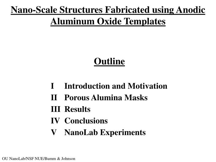
Nano-Scale Structures Fabricated using Anodic Aluminum Oxide Templates. Outline. I Introduction and Motivation II Porous Alumina Masks III Results IV Conclusions V NanoLab Experiments. Introduction. Objective:.

E N D
Nano-Scale Structures Fabricated using Anodic Aluminum Oxide Templates Outline I Introduction and Motivation II Porous Alumina Masks III Results IV Conclusions V NanoLab Experiments
Introduction Objective: Fabricate ordered arrays of structures on the nanometer scale using porous alumina templates.
Integrated Circuits Moores Law: • Dr. Gordon E. Moore, founder of Intel, predicted in 1965 that the number of transistors per IC doubles every 18 months. http://www.intel.com/research/silicon/mooreslaw.htm
Semiconductor Roadmap Important characteristics of “The 1999 National Technology Roadmap for Semiconductors” published by the SIA. • Current technology hits a roadblock in about 2012 in terms of fabrication and device operation. • Alternative patterning techniques and computing schemes are needed (e.g. Quantum, Molecular, Optical Computers, Carbon Nanotubes based devices, etc.).
Motivation: General What is Anodic Porous Alumina? • Aluminum oxide grown on an Al substrate in an electrolytic cell. The resulting structure consists of an array of tunable nanometer-sized pores surrounded by an alumina backbone. Purpose: • To understand the mechanisms involved in the growth and ordering of anodic porous alumina. Motivation: • Interest in using anodic porous alumina as a nano- template to fabricate nanometer-sized structures (e.g. nanofabrication of quantum dots). Why do we want to fabricate nanostructures? • 1. Fundamental physical interest in the nanometer size regime. Properties of nano-sized structures are different from their bulk and molecular counterparts. • 2. Technological applications as electronic and optical devices.
Motivation: Applications Commercially available Anopore filter. http://www.2spi.com/catalog/spec_prep/filter2.html 1. Physics: • Explore optical, electrical, and magnetic quantum confinement. 2. Engineering: • Microfiltration. • Optical waveguides and photonic crystals for optical circuits. • Template for carbon nanotube growth for electronic, mechanical applications. • Ordered arrays of quantum dots for lasers, photodetectors. • ULSI memory devices and ICs. Porous Alumina used as optical waveguide. H. Masuda, et. al., Jpn. J. Appl. Phys.38, L1403 (1999). Ordered arrays of carbon nanotubes fabricated using a porous alumina template. J. Li, et al., Appl. Phys. Lett. 75(3), 367 (1999).
Overview of Anodic Oxide Films Fabrication • Anodizealuminum in electrolyte (e.g. Oxalic Acid) Two main types of anodic oxide films can be grown depending on the nature of the electrolyte: • 1. Barrier-Type Films: • Grown Oxide Insoluble in Electrolyte • Nearly Neutral Electrolytes (pH 5-7) • 2. Porous-Type Films: • Grown Oxide Slightly Soluble in Electrolyte • Aqueous Sulfuric, Oxalic, and Phosphoric Acid Electrolytes
Historical Timeline • 1920’s Porous alumina starts to be used commercially to protect and finish bulk Al surfaces. • 1940’s-1960’s With advent of electron microscopes, first characterization of structure of porous alumina, but growth theories are experimentally unsubstantiated. • 1970 Manchester group does first real experimental work showing pore radius dependence on applied voltage,etc. • 1992 First “quantitative” theoretical attempt to explain pore growth from first principles by Belorus group. • 1995 Japanese group discovers pores will self-order into close packed array under the right anodization conditions. • 1996-Present Use of porous alumina for nano-applications abound. • 1998 Although mechanism for ordering still not clear, German group proposes one possible mechanism.
Porous Alumina Apparatus • Anodize aluminum in electrolyte (e.g. Oxalic Acid). • Oxide grows at the metal/oxide and oxide/electrolyte interfaces, pores initiate at random positions by field-assisted dissolution at the oxide/electrolyte interface. • Ordering requires appropriate potentials and long anodization times. • Ordering results from repulsion between neighboring pores due to mechanical stress at the metal/oxide interface. Resulting Structure H. Masuda and K. Fukuda, Science268, 1466 (1995).
Barrier-Type Anodic Oxide Films Growth Mechanism • Oxide growth proceeds at the Aluminum anode (+). • Hydrogen gas is evolved at the Platinum cathode (-). • The current between the cathode and anode is carried by the electrolyte. • Oxidation reactions at the Al anode • Electrolysis of water at aluminum oxide/ electrolyte interface • Reduction reaction at the cathode: • The overall electrochemical reaction occurring is:
Barrier-Type Anodic Oxide Films Growth Mechanism • Oxide growth proceeds at the metal/oxide and the oxide/electrolyte interface. • Growth proceeds due to the motion of ions under the applied field. • Growth at the metal/oxide interface is due to oxygen containing anions (mainly OH- and O2-) moving through interstitial/vacancy sites. • Growth at the oxide/electrolyte interface is due to Al3+ cations moving through interstitial/place exchange mechanisms.
Overview of Film Anodization • Oxide growth proceeds via ionic conduction and reaction of Al cations and oxygen containing anions under the influence of an applied field. (e.g. 2Al+ + 3OH- Al2O3+3H++6e-) • Pores initiate at random positions through field-assisted dissolution of the oxide at the oxide/electrolyte interface. • Initially oxide growth dominates. (I) • Dissolution becomes competitive, barrier layer thins, and pores initiate. (II) • Approaches steady state where both mechanisms occur at roughly the same rate. (III and IV) V.P. Parkhutik, and V.I. Shershulsky, J. Phys. D:Appl. Phys.25, 1258 (1992).
Porous-Type Anodic Oxide Films Field-Assisted Dissolution • Application of a field across the oxide polarizes the oxide bonds. • This polarization effectively lowers the activation energy for dissolution of the oxide. • This promotes solvation of Al3+ ions by water molecules and the removal of O2- ions by H+ ions. • This processes is strongly dependent on the E-field strength.
Ordered Growth of Porous Alumina • In 1995, Japanese group found that pores will self-order under the right anodization conditions. • The two most important conditions are narrow voltage ranges and long anodization times.
Ordered Nano-Templates Ordered Oxalic Near-Ordered Sulfuric • Tunable diameters and spacings from 20 nm to 500 nm. • Polycrystalline structure: ordered micron-sized domains, defects at grain boundaries. • Low temperature growth produces unordered 4-10 nm arrays.
Ordered Growth of Porous Alumina • Ordered pore arrays obtained in three different electrolytes for long anodization times and appropriate voltages (specific for each electrolyte). • Polycrystalline structure with perfectly ordered domains a few microns in size. Defects occur at grain boundaries.
Mask Processing To create an ordered through-hole mask: 1. Anodize for a long time allowing pores to order. 1. 2. Chemically remove the alumina in a mixture of phosphoric and chromic acid. AFM of Unopened Barrier Layer (1 mm x 1 mm) 2. 3. Anodize for a short time (now pores are ordered). 3. 4. Coat top surface of alumina with a polymer (collodion) to protect it from further processing. 4. 5. Remove Al Substrate in a saturated HgCl2 solution. 5. 6. Remove the barrier layer in 5 wt.% Phosphoric Acid. 6. 7. Remove collodion and place alumina on desired substrate. 7. H. Masuda et al. , Jpn. J. Appl. Phys. 35, L126 (1996).
Pattern Transfer Techniques: Results 1. Etching Processes Fluorine Beam Transfer mask pattern via etching into substrate for ordered arrays of trenches. Ion Beam Transfer mask pattern via ion etching into substrate for ordered arrays of trenches or pillars. 2. Growth Processes Sputtering and Thermal Deposition Transfer mask pattern via deposition onto substrate for ordered arrays of dots.
F-Etched Array of Si(001) Nano-Holes 50 nm 200 nm SAMPLE: ~500nm thick Free-Standing AAO/Si(001) F-ETCH: 1 min. 20 sec. TSUB = 250oC PORES: Width 70 nm, Depth 100-120 nm TOP DOWN VIEW X-SECT. VIEW • Walls are ~30 nm thick (near top).
Ion Etched Array of GaAs Nano-Holes SAMPLE: ~500nm thick Free-Standing AAO/GaAs(100) ION BEAM: 500 eV Ar+, 0.05 mA/cm2 Time = 2hrs. 12min. PORES: Width 50 nm, Depth 50-60 nm OBLIQUE VIEW ~TOP DOWN VIEW X-SECT. VIEW
Thermally Evaporated Nano-Dots: MgF2 200 nm Line Scan SEM Top Views MgF2 dots/Si Au dots/SiO2 AFM Views 3-D Rendered Height: 12 nm ± 11% Diameter: 60 nm ± 9% Spacing: 110 nm ± 5%
Thermally Evaporated Nano-Dots: Gold • Porous alumina used as an evaporation mask to grow quantum dots. H. Masuda et al. , Jpn. J. Appl. Phys. 35, L126 (1996).
Ion Etched Array of GaAs Nano-Pillars SAMPLE: ~20nm thick Fe dots on GaAs(100). ION BEAM: 500 eV Ar+, 0.05 mA/cm2 Time = 17 min. PILLARS: Width 50 nm, Height 50 nm OBLIQUE VIEW TOP DOWN VIEW X-SECT. VIEW Note: No Fe remaining.
Evaporated Catalyst Dots For Carbon Nanotube Growth SAMPLE: ~20nm thick Fe catalyst dots on 100nm Ti/Si GROWTH: CVD using Methane gas at 500 Torr, 800oC NANOTUBES: Multi-walled tubes, ~10s of microns long TOP DOWN VIEW • Collaboration with Dr. Shen Zhu of Marshall Space Flight Center.
Conclusions Fabricated ordered, arrays of nanostructures using porous alumina templates as masks: • Arrays of 50 nm wide trenches in Si and GaAs by atom-beam and sputter etching. • Arrays of 50 nm dots of various materials onto substrates by evaporation and sputtering. • Arrays of nano-pillars in Si and GaAs by etching nano-dot arrays. Future • Make pores smaller (to 5 nm) using sulfuric acid electrolytes and low temp. anodization. • Seed for carbon nanotube growth. • Explore optical, electrical, and magnetic properties of nanostructures. • Explore ways to transfer single or arbitrary dot/trench patterns. • Fabricate such nanostructures in situ in multichamber MBE system.
NanoLab Class: AAO Templated Structures • Fabricate AAO Masks: • Ordered and Disordered Oxalic Masks (50 nm/100 nm). • Ordered film: 15 hr first anodization. • Disordered film: 1 hr first anodization. • Lift-Off onto Silicon and Quartz substrates. • Silicon substrates for SEM characterization. • Quartz substrates for UV-Vis characterization. • Thermally Evaporate Gold onto all Samples • Must be done one sample at a time, because alignment is critical. • Characterize Samples • AFM -both samples • SEM of Au dots on Silicon. • UV-Vis of Au dots on Quartz.