Download
1 / 43
460 likes | 677 Views
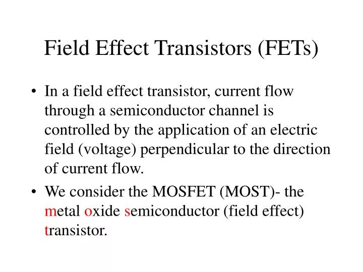
Field Effect Transistors (FETs). In a field effect transistor, current flow through a semiconductor channel is controlled by the application of an electric field (voltage) perpendicular to the direction of current flow.

E N D
Field Effect Transistors (FETs) • In a field effect transistor, current flow through a semiconductor channel is controlled by the application of an electric field (voltage) perpendicular to the direction of current flow. • We consider the MOSFET (MOST)- the metal oxide semiconductor (field effect) transistor.
Field Effect Transistors (FETs) • In a depletion mode MOSFET a channel is built in so that conduction occurs with no control voltage applied. • We consider an n-channel enhancement mode device which has no ‘built-in’ conduction channel.
Oxide (SiO2) Gate (G) Drain (D) n+ n+ p-type silicon N-channel enhancement mode MOSFET (schematic) Source (S)
Symbol for N-channel enhancement mode MOSFET • Note connection to substrate shown
D G S Symbol for N-channel enhancement mode MOSFET • Note connection to substrate shown
N-channel enhancement mode MOSFET: outline of operation • VGS =0, little or no current can flow S D, back to back p-n junctions. • As a positive VGS is applied , holes in the p-region are repelled. • As VGS increases further, electrons are attracted from the substrate towards the positive gate. • An inversion layer of mobile electrons forms near the silicon surface.
Oxide (SiO2) Gate (G) Drain (D) n+ n+ Inversion layer (conduction channel) p-type silicon N-channel enhancement mode MOSFET with inversion layer Source (S)
N-channel enhancement mode MOSFET: outline of operation • This inversion layer is effectively n-type. • Electrons can carry current in an continuous n-type path (or channel) from source to drain. • The conduction channel forms when VGS attains a threshold voltage, VT
N-channel enhancement mode MOSFET • The value of VT is determined by the device process and the level of the p-type (substrate) doping. • Note that an n-channel device is formed with a p-type substrate.
N-channel enhancement mode MOSFET • As VGS increases further, more electrons are drawn into the inversion layer and the channel resistance decreases (The device operates as a voltage controlled resistor). • However……
N-channel enhancement mode MOSFET • The voltage between gate and channel varies from VGS at the source end to VGS -VDS at the drain end. • Thus as the voltage at the drain end, VDS , is increased the effective gate-channel voltage (vertical field) is decreased.
N-channel enhancement mode MOSFET • This causes the carrier density at the drain end of the inversion layer to decrease. • The current levels off or saturates. • The FET is then said to have entered its saturation region (This expression had a different meaning in our discussion of BJTs).
N-channel enhancement mode MOSFET • The boundary where saturation starts occurs at (VGS –VDS ) = VT. i.e. VDS = (VGS – VT) • Ideally we would want a further increase in VDS to have no effect on the drain current ID
N-channel enhancement mode MOSFET • In practice as VDS is increased further ID also increases. • This is due to a reduction in the effective channel length with VDS . • We note, for design purposes, that the gate current (IG) is effectively zero. (We have an insulating oxide region)
N-channel Depletion mode MOSFET • In a depletion mode MOST a channel is built into the device. • Conduction occurs at VDS = 0. • (The threshold voltage VT is negative)
Symbol for N-channel depletion mode MOSFET • Connection to substrate shown. • The solid line indicates that a physical channel exists at VGS =0.
P-channel devices • These are widely used, particularly in Complementary MOS (C-MOS) circuits. • Electron mobility is larger than hole mobility so n-channel devices are faster, i.e. they have a higher frequency response.
VDS = VGS - VT Plots and Equations, Enhancement mode, VT 2 V
FET Plots and equations • The FET is a voltage controlled device. • The ‘control parameter’ is VGS –compare with IB in the BJT.
FET Drain Source Gate BJT Collector Emitter Base Loose equivalences
VDS = VGS - VT Plots and Equations Saturation region
VDS = VGS - VT Plots and Equations ‘Triode’ region
ID VT VGS Transfer Characteristic • Gives the relationship between ID and VGS in the saturation (constant current) regime. • e.g. for an enhancement mode device
Transfer Characteristic • This I-V curve in the saturation region can be approximated by the parabola • This equation is very important! • The ID-VGS relationship is not a linear one!
Transfer Characteristic • K is a device parameter whose value is typically 0.25mA/V2
Detailed analysis shows that L = channel length, W = channel width, e = electron mobility and Cox is the capacitance per unit area formed by the the gate-oxide- substrate Transfer Characteristic
Transfer Characteristic • We could allow for channel length modulation by including a small linear dependence of ID on VDS in the saturation region.
Small Signal Model • In the saturation region we can model the square law device by a linear small signal equivalent circuit. • (Although the device characteristic is a parabola we approximate it by a straight line for small signals)
Ig0 G D id vgs gmvgs vds S FET Small Signal Equivalent Circuit
ig0 G D id vgs gmvgs vds S FET Small Signal Equivalent Circuit • Channel length modulation makes the output resistance in saturation finite r0
Bias Circuit A: Voltage Divider Bias • Remember IG = 0 VDD R1 RD ID = IS D IG S G R2 VGG RS IS = ID GND
Bias Circuit A • Solve VGS = VGG – IDRS • with • to give:
Bias circuit A • This is a quadratic equation for ID. • Usually one solves for ID then for VGS and determines the small signal transconductance gm as
Bias circuits • We note that gm is determined by the d.c. bias condition in much the same way as the dynamic resistance r was for the BJT.
Bias circuit B (Drain Feedback Bias) VDD RD ID RG ~ 100M IG = 0 IS ~ ID GND
Bias circuit B • IG = 0 • VGS ~ VDS • VDD-RDID- VDS =0 • For fixed supply VDD, an increase in ID means VDS decreases. This corresponds to a decrease in VGS which tends to decrease ID via • RG is large to minimise current flow from output back to input (we assume IG = 0).
Common Source Amplifier • Same procedure as for BJT but using the simpler FET small signal equivalent circuit • Remember the FET has Zin= and id = is ig0 id G D vgs gmvgs vds S
For Example: Common Source Amplifier with Bias Circuit A VDD R1 RD vout R2 RS vi GND
G vin R1//R2 vgs For Example: Common Source Amplifier with Bias Circuit A D id RD gmvgs vds S