Download
1 / 27
270 likes | 473 Views
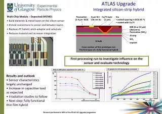
Design and Simulation of Silicon Strip Sensor. 배재범 (KNU). Contents. Physical Mechanism Silicon strip sensor design Design Tool – Cadence Silicon sensor parameters DSSD (Double-sided strip detector) design : N-type & P-type Silicon strip sensor simulation ATHENA & ATLAS. 0V.

E N D
Contents • Physical Mechanism • Silicon strip sensor design • Design Tool – Cadence • Silicon sensor parameters • DSSD (Double-sided strip detector) design : N-type & P-type • Silicon strip sensor simulation • ATHENA & ATLAS
0V N+ - - Depletion Region - - - + + + + + P+ -85V Physical Mechanism • Depletion region is made by reverse bias. • If energetic particle passesthrough the DSSD, energeticparticle makes electron and hole pair. • Electron moves towards N strip and hole moves towards P strip by the reverse bias. Energetic particle
Design Tool • Cadence (운영체제:Solaris) • Cadence Tool은 EDA환경의 front-end로부터 back-end까지 Full-line으로 IC설계 Tool을 제공. • ASIC, structured custom IC, digital-analog mixed IC, 그리고 analog IC 등 IC 설계의 Front에서 Back까지 Framework 환경하에서 설계/개발 수행이 가능.
DSSD Schematics • 양면에 각각 511개의 Readout Channel을 두고 Implanted Strip은 서로 직교가 되도록 설계 n+ ohmic side 1st metal 2nd metal readout line p+ junction side Metal 1 and metal 2 contact (VIA) • Readout을 같은 방향이 되도록 하기 위해 P-Side에 Implanted Strip(1st Metal)과 직교하는 Readout Metal(2nd Metal)을 추가
N-side Design 64ch 50um pitch sensor 511ch 50um pitch sensor 32ch 50um pitch sensor 1cm PIN Diode 16ch 50um pitch sensor For SDD R&D PIN Diode array Backside of SSD
N-side : Sensor P-Stop Guard ring Pad Readout P-Stop 512ch 50um pitch sensor
P-side Design 64ch 100um pitch sensor 511ch 100um pitch sensor Without hour glass (Sensor 1) 1cm PIN Diode 16ch 100um pitch sensor 32ch 100um pitch sensor For SDD R&D PIN Diode array 511ch 100um pitch sensor With hour glass (Sensor 2) 16ch 100um pitch SSD
P-side : Sensor 1 모래시계모양으로 implant 511ch 100um pitch sensor • Implant와 Metal이 직교한다. • Cap을 줄이기 위한 디자인 • Double-metal structure
P-side : Sensor 2 일정한 두께로 implant 511ch 100um pitch sensor • Hourglass 디자인이 공정상 어려움을 보안한 디자인 • 기존의 디자인에 추가된 부분
Simulation Tool • TCAD (Technology CAD) • 실제 제작 없이 주어진 Model을 이용하여 그 구조와 특성을 예측하는 것 • 반도체 공정, 소자 Simulation • ATHENA process technology simulators • ATLAS device technology simulators
Simulation Tool • ATHENA ( Process Simulation Framework ) • 공정 순서에 따른 구조 변화 • Impurity Implantation과 Diffusion에 의한 Doping Profile 변화 • Oxidation에 의한 Oxide Profile 변화 • Deposition, Etching등으로 인한 모양의 변화 • Oxidation, 열팽창 등에 의한 Mechanical Stress 분포 • ATLAS( Device Simulation Framework ) • (공정 Simulation으로) 결정된 구조의 전기적 특성 • Transistor의 Voltage-Current 특성 • Transistor 내부의 Potential, Electric Field, Carrier 분포
ATHENA (Process Simulation Framework ) Oxidation Etching & Nitride Devise Implantation
Device Structure N-type Si , >5 kohm, 380um
ATLAS( Device Simulation Framework ) Leakage current IV curve Potential CV curve
Summary • 1st sensors were fabricated and measured • 2nd Sensor/Mask Designs with feedback are done • 단위공정을 위한 simulation을 마치고 테스트 함 Thank you~!
Via 2nd Metal Via 2nd Metal 1st Metal SiO2 1st Metal SiO2 P+ P+ Contact Contact Contact & Via 이곳을 단면으로 한 공정의 변화 변경전 : Contact과 Via가 같은 자리에서 공정된다. 변경후 : Contact과 Via가 엇갈려 공정된다.
R&D Patterns • 16, 32, 64채널로 같은 센서를 제작하여 채널수에 따른 센서의 특성을 조사한다. PSIDE :16ch 100um pitch Sensor • 실제 센서의 경우 채널수가 많아 한번에 측정이 어려움을 감안하여 채널수를 줄인 센서 설계 NSIDE :16ch 50um pitch Sensor
1st Metal Contact SiO2 p+ 2nd Metal SiO2 Via Test Patterns : PSIDE-SSD 양면 Sensor의 공정에서 PSIDE의 경우, Metal 공정이 두번 있어 한면 Sensor의 경우에도 Metal을 고려하여 디자인을 하였다. 16ch 100um pitch sensor(55610X5560) Metal P+ Implant보다 contact을 작게해서 metal을 더 크게 올렸다. p implantation p implantation Contact은 유지하고 P+ Implant 보다 metal을 더 작게 올렸다. Metal
Test Patterns : Pixel array • Pixel의 크기는 25um☓25um, 50um☓50um, 100um☓100um이고, 각각을 5☓5로 배열 • 측정시 Wire Bonding을 편하게 하기 위하여 Pad를 따로 만들어 준것을 추가 각각의 diode마다 직접 bonding 각각의 diode에 readout pad를 만들어서 bonding
Test Patterns : SDD R&D 1 • Silicon Drift Detector R&D를 위한 Pattern • Guard ring을 포함한 크기 : 1cm☓1cm • NSIDE에 센서를 두고 뒷면은 무공정 • 센서의 배열에 따라 세종류가 있다. 50um☓50um n implantation 100um☓100um Metal
Test Patterns : SDD R&D 2 • 크기는 동일 • 센서외의 공간을 p implant로 채운다. • PSIDE에도 p implant로 전체를 채운다. 50um☓50um n implantation 100um☓100um Metal
Al Al SiO2 e-accumulation n+ strip N-type wafer Insulation problem for n+ strip in silicon, due to electrical shortening by the electron accumulation layer.
Al Al n+ strip p-stop (atoll design)