Download
1 / 33
330 likes | 345 Views
This workshop presentation discusses the motivations for using pixelized readout in Time Projection Chambers (TPCs), the use of Medipix2 and TimePix chips in TPCs, and the progress and potential applications of this approach. Topics covered include spatial resolution, high granularity, direction and energy of tracks, and the use of CMOS pixel detectors with gas amplifier grids.

E N D
Digital TPC TimePix David Attié MPGD Workshop in Saga, Japan – 27 January 2007 MPGD Workshop in SAGA, Japan – January 27, 2007
Summary • Motivations for a pixelized readout TPC • From Medipix chip to TimePix chip • Integrated Grid: InGrid • Micromegas & GEM detectors for digital TPC • First results • Work in progress and possible applications MPGD Workshop in SAGA, Japan – January 27, 2007
Motivations for pixel readout of TPCs wire Cathode pads GEM Micromegas Why a digital readout TPC ? • Spatial resolution: • σxy limited by the pad size (pitch/√12) • Narrow charge distribution (RMS ~15 μm) • High granularity: • δ-ray recognition/suppression in TPC • Direction & energy of tracks: • low-energy e- for X-ray polarimetry • nuclear recoils in WIMP or neutrino interactions • 2 e- from double beta decay • Possibility to count primary clusters & electrons • A novel approach for the readout of a TPC is to use a CMOS pixel detector combined with a gas amplifier grid SiTPC Using a naked photon counting chip Medipix2 coupled to GEMs or Micromegas demonstrated the feasibility of such approach MPGD Workshop in SAGA, Japan – January 27, 2007
The Medipix2 chip • Hybrid pixel detector (CMOS ASIC) developed by the Medipix consortium (CERN) for medical applications • Chip layout: • 1.4 x 1.6 cm2 area • 256 x 256 pixel matrix • 55 x 55 µm2 pixels • On each pixel: • Preamplifier + shaper • 2 discriminators (thresholds) • 14-bit counter • Smaller input noise (Cin ~ 15 fF) • Lower gain, less aging, smaller ion backflow • Small charge sensitivity • Single electron detection with an efficiency depending on the gain and the amplification structures Low threshold ~ 1000 e- 55 mm The chip is used as the detector anode MPGD Workshop in SAGA, Japan – January 27, 2007
The Medipix2 chip 14.11 mm 2.53 mm 55 μm MPGD Workshop in SAGA, Japan – January 27, 2007
Medipix2 & Micromegas DRIFT DRIFT SPACE ED ~ 1 kV/cm 14.08mm MICROMEGAS Medipix2 READOUT • Micromegas mesh of 50 mm of gap • Gas mixture: He/Isobutane 80/20 • Efficiency for detecting single electrons: > 90 % • δ-ray seen ! 15 mm 50 mm Vm ~ -400 V NIKHEF Saclay (2004) AMPLIFICATION SPACE EA ~80 kV/cm MPGD Workshop in SAGA, Japan – January 27, 2007
Medipix2 & Micromegas He 20% iC4H10 Ar 20% iC4H10 Larger diffusion Top of track NIKHEF Saclay (2004) Helium vs. Argon mixtures: • Argon: larger primary statistic & transverse diffusion • Clusters and single electrons have been observed Excellent tool to study ionization statistic of photons & charged particles … MPGD Workshop in SAGA, Japan – January 27, 2007
Medipix2 & GEM s ~ 55 mm 14.08mm 14.08mm • Drift chamber of 6 mm drift gap filled with 70/30 Ar/CO2 gas mixture • Typical 106Ru-event (beta source): - Noise reductionby removing isolated pixels - Cluster finding by looking for contiguous connected areas using a linear track fit to cluster centers Freiburg (2005) 6 mm 2 mm 2mm 1 mm Medipix2 DVGEM ~ -400 V MPGD Workshop in SAGA, Japan – January 27, 2007
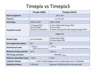
From Medipix2 to TimePix • These experiments (by NIKHEF/Saclay, Freiburg 2004/2005 ) demonstrated that single electrons could be detected using a naked Medipix2 chip 2D • But no information on the arrival time or the energy of the electron in the sensitive gas volume 3D not available but needed for a TPC • A new chip using the Medipix2 structure has been redesigned to integrate a time stamp with a tunable resolution of 10 to 100 ns TimePix chip • Requirements: • Keep TimePix as similar as possible to Medipix2 in order to benefit from large prior effort in R/O hardware and software • Avoid major changes in pixel and/or readout logic – risk of chip failure due to poor mixed mode modeling • Eliminate 2nd threshold • Add possibility of programming pixel by pixel arrival time or TOT information MPGD Workshop in SAGA, Japan – January 27, 2007
The history • TimePix Proposal in November 2004: • develop • produce Medipix2 TimePix • test • Starting 2006, EUDET: Detector R&D towards the International Linear Collider http://www.eudet.org/ • TimePix test at CERN ~ November 2006 MPGD Workshop in SAGA, Japan – January 27, 2007
TimePix test at Cern • Chip design was submitted to foundry (IBM) on the beginning of July 2006 • 12 wafers (of 100 chips) delivered to CERN 2nd week of September 2006 • Between September to December half wafers has been tested following • some specific procedure using a probing bench: • - analogic tests (TOT & Medipix modes) • - digital tests using calibration of DACs 80 % of good chip has been found ! MPGD Workshop in SAGA, Japan – January 27, 2007
TimePix Layout status Timepix layout Mpix2MXR20 layout 1: Preamplifier; 2/3: Threshold discriminator; 4: 8-bit configuration latches 5; Disc., 6: 14-bit Counter and overflow control MPGD Workshop in SAGA, Japan – January 27, 2007
TimePix Schematic Previous Pixel For each pixel Ref_Clkb Clk_Read Mux 4 bits thr Adj Mask Mux Preamp Input Disc 14 bits Shift Register Shutter Timepix Synchronization Logic THR Shutter_int Ctest P0 Conf Testbit Polarity P1 8 bits configuration Test Input Ovf Control Ref_Clk Clk_Read Next Pixel Digital Analog MPGD Workshop in SAGA, Japan – January 27, 2007
TimePix chip architecture • IBM 0.25 µm process technology • Chip architecture almost identical to Medipix2 (MXR20) • 256x256 pixels of 55µm square • Analog Power -> 440mW • Digital Power (Ref_Clk=50MHz) -> 220mW • Serial readout (@100MHz) -> 9.17 ms • Parallel readout (@100MHz) -> 287 µs • > 36M Transistors MPGD Workshop in SAGA, Japan – January 27, 2007
TimePix synchronization logic control Medipix Mode Timepix Mode TOT Mode not detected detected Charge summed • Each pixel can be configured independently in 5 different modes • Internal clock up to 100 MHz 100 MHz MPGD Workshop in SAGA, Japan – January 27, 2007
InGrid: Integrated GEM/Micromegas Grid • Integrate GEM or Micromegas detector and pixel readout chip… • … by wafer post-processing technology: Grid Grid Walls Pillars Si Wafer + GEM Si Wafer + Micromegas Deposit SU-8 ~50 mm Deposit anode ~200 nm of Al Deposit metal ~1 mm of Al UV exposure NIKHEF Twente Univ. Pattern metal Develop resist MPGD Workshop in SAGA, Japan – January 27, 2007
InGrid: Integrated Grid InGrid on top of pixel matrix Grid hole centered between 4 pixels pillars pixels • Wafer post-processing advantages: - Low temperature process: spin coating, wet etching; - Perfect alignment between grid holes and pixel pads; - No dead areas due to pillars; - Flexible design (a few 10 mm). • First trials promising on Medipix2 (using rejected chips): MPGD Workshop in SAGA, Japan – January 27, 2007
InGrid: field structure 10 cm Wafer thickness: 300 mm No chip MPGD Workshop in SAGA, Japan – January 27, 2007
InGrid studies Gain 60 104 40 FWHM (%) 103 30 20 102 460 420 540 Vgrid (V) 500 10 Gain 103 104 Three examples of field structure for 75 mm of gap: Resolution minimum (13 %) at: G ~ 5.103 No grid geometry dependency Gain dependency with the optical transparency MPGD Workshop in SAGA, Japan – January 27, 2007
Maximum predicted in gain M vs gap d: InGrid: gain for different gap sizes Gain 10000 V=400Volts 1000 V=350Volts 100 V=300Volts 105 500V 40 mm 10 450V 55 mm 1 400V 35 mm 0.001 0.1 0.01 1 Gap (mm) 75 mm 104 Gain 103 102 65 35 55 75 45 300 380 460 540 Gap thickness (μm) Grid voltage p pressure A,B depend on gas mixture d gap thickness Y. Giomataris et al.,N.I.M. A419 (1998) 239-250 • Measurements are possible now using InGrid: MPGD Workshop in SAGA, Japan – January 27, 2007
InGrid: gain & resolution measurements • 55Fe source + gas mixture: Helium/iC4H10 80/20 • Observation of two lines: • Kα at 5.9 keV • Kβ at 6.4 keV • Gas gains: 103 - 6∙104 hexagonal holes (pitch 60 μm) (diameter of pillars 30 μm) gap of 50 μm (standard MM) M. Chefdeville et al., N.I.M. A556 (2006) 490-494 MPGD Workshop in SAGA, Japan – January 27, 2007
InGrid: gain & resolution measurements • 55Fe source + gas mixture: Argon/iC4H10 80/20 • Observation of two lines well-separated: • Kα at 5.9 keV • Kβ at 6.4 keV • Resolution: σE/E = 6.5% (FWHM = 15.3%) • Gain variations: < 5% • Gas gains: 5∙102 - 6∙103 hexagonal holes (pitch 60 μm) (diameter of pillars 30 μm) MPGD Workshop in SAGA, Japan – January 27, 2007
InGrid: spark issue • Amplification by high voltage: - ~ 80 kV/cm - sparks could kill the chip Solutions: • High resistivity layer (RPC principle) - cover the chip with it will reduce locally the E field - limit maximum avalanche no spark anymore • Two/Three-stage Ingrid structure using a wafer post-processing technique (Twin or Triple Ingrid) MPGD Workshop in SAGA, Japan – January 27, 2007
TimePix & Micromegas 14.08mm 14.08mm Preliminary results (December 2006): • TimePix chip covered by 4 mm of amorphous Silicon (aSi) with resistivity of ~1011.cm • Small drift chamber (15 mm drift gap) filled with 80/20 He/Isobutane gas mixture • Grid HV is at -400 V (gain ~8500) since December 18th 2006 without sparks • Electron tracks of a beta emission from 90Sr source in "time-over-threshold" mode • • Tracks from cosmics triggerred by three scintillators during a time windows of 700 s MPGD Workshop in SAGA, Japan – January 27, 2007
TimePix & GEM The larger the number of counts, the shorter the drift time Test beam in DESY (November 2006): • 6 mm long drift chamber for 3 GEM (2, 2, 1) • Every fired pixel counts till the end of a 12 μs shutter window • Tracks parallel to the pixel plane (same color) Timepix mode MPGD Workshop in SAGA, Japan – January 27, 2007
TimePix & GEM • Consecutive pixels have Time and TOT assignment and are here separated via mapping onto a 181x181 matrix • Provide charge & time information in the same time • Very interesting for double track separation Ar CO2 70/30 He CO2 70/30 MPGD Workshop in SAGA, Japan – January 27, 2007
Future development + Medipix2/TimePix Micromegas • no ExB effect • good for 2-track separation • high gain • very fast electron signal on the • anode plane • small ion feedback in the drift • space • robust and easy to implement • only one power supply is needed • 55 mm pixels • Direct X-ray conversion • Low noise • 14-bit counter per pixel Mini-chamber SiTPC endplate+Large Prototype For ILC MPGD Workshop in SAGA, Japan – January 27, 2007
Box design • First test of a Medipix2 + Micromegas in the gas • Improve the gas mixture (“non-sparking” operation) • Medipix2 TimePix readout chip LP endplate Metallic box of 24 cm x 14 cm x 6 cm size M. RIALLOT (DAPNIA/SEDI) MPGD Workshop in SAGA, Japan – January 27, 2007
Mini-chamber for the Medipix2/TimePix chip Design plan: Windows for X-rays source Box 2.5 cm 6 cm Windows for b source Field cage Micromegas mesh M. RIALLOT (DAPNIA/SEDI) Medipix2 readout chip MPGD Workshop in SAGA, Japan – January 27, 2007
Further Tests and Developments • Investigate possible use of CMS (or Atlas) front-end pixel chip • Chip tiling: large(r) detector surfaces (2x2, 2x4 chips) • Through Si connectivity: avoiding bonding wires and dead space (RELAXD) • Fast readout technology (~5 Gb/s) NIKHEF, Panalytical, IMEC, Canberra MPGD Workshop in SAGA, Japan – January 27, 2007
SiTPC as X-ray Polarimeter X-ray E f Auger electron Photoelectron • Based on: correlation between the X-ray electric field vector and the photoelectron emission direction (L=1) • Ideal polarimeter is an track imagerwith: the photo-electric effect • is the most useful physical process because the cross section • is largest at energies of less than 20 keV • To obtain the polarization angle, the photo-electron • (which is ejected in the polarization direction with the • maximum probability) is tracked. • A micro-pattern gas detector using TimePix+Ingrid, • is a good candidate for x-ray polarimeter. MPGD Workshop in SAGA, Japan – January 27, 2007
Conclusions • * TimePix chip is a good candidate for a digital TPC, only limited by diffusion ! • Could be used for the future International Linear Collider (SiTPC) • and also for others experiments using TPC (polarimetry, WIMP, etc..) • * Test to be continued in the next weeks using both GEM and Micromegas to improve the TimePix technology • * Excellent tool for gas properties studies • Medipix is an industrial consortium which implies dealing with Intellectual Property … Bonn K. Desch, P. Wienemann, M. Killenberg. CEA/Saclay/David Attié, Dan Burke, Paul Colas, DAPNIAArnoud Giganon, Yannis Giomataris, CERNMichael Campbell, Erik Heine, Xavi Llopart, NIKHEFMaximilien Chefdeville, Martin Fransen, Harry van der Graaf, Jan Timmermans, Jan Visschers, Univ. Twente/Jurriaan Schmitz, Cora Salm, Mesa+Victor Blanco Carballo, Sander Smits, Freiburg A. Bamberger, U. Renz, M. Titov, N. Vlasov, A. Zwerger. Thanks to: Wim Gotink Joop Rovenkamp Marc Riallot MPGD Workshop in SAGA, Japan – January 27, 2007
The end 有難う MPGD Workshop in SAGA, Japan – January 27, 2007