Download
1 / 42
420 likes | 693 Views
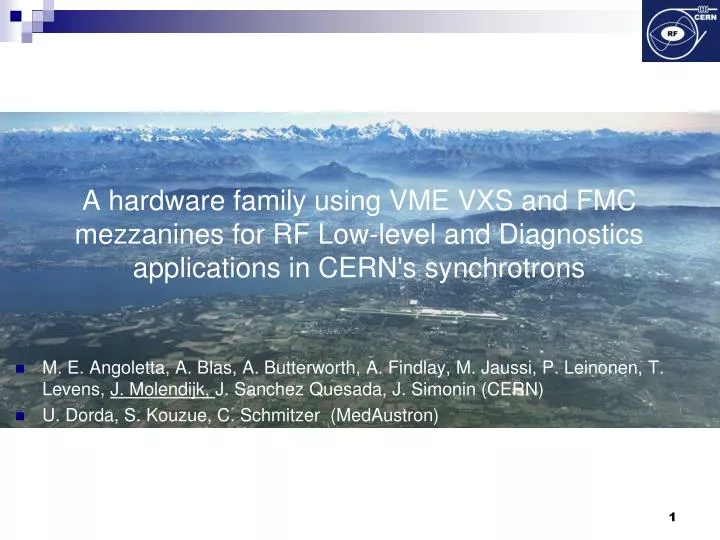
A hardware family using VME VXS and FMC mezzanines for RF Low-level and Diagnostics applications in CERN's synchrotrons. Maria-Elena Angoletta , Alfred Blas, John Molendijk CERN BE/RF Jorge Sanchez Quesada MedAustron Petri Leinonen Fellow.

E N D
A hardware family using VME VXS and FMC mezzanines for RF Low-level and Diagnostics applications in CERN's synchrotrons Maria-Elena Angoletta, Alfred Blas, John Molendijk CERN BE/RF Jorge Sanchez Quesada MedAustron Petri Leinonen Fellow • M. E. Angoletta, A. Blas, A. Butterworth, A. Findlay, M. Jaussi, P. Leinonen, T. Levens, J. Molendijk, J. Sanchez Quesada, J. Simonin (CERN) • U. Dorda, S. Kouzue, C. Schmitzer (MedAustron)
Introduction 1 See poster ID#46 LLRF2013 «LLRF & Longitudinal Diagnostics Implementation for CERN’s ELENA Ring» J.C. Molendijk – GSI meeting 2014 • A DSP based digital LLRF developed around 2003 at CERN using a BNL developed motherboard and CERN developed daughter cards and other modules has been successfully used to operate LEIR at CERN since 2005 [1,2,3,4] • A Novel hardware family for LLRF and diagnostics1 applications in CERNs synchrotrons has now been developed to succeed this previous (prototype) generation. • Similar from a conceptual viewpoint • Entirely redesigned using recent components • Adheres to recent industry standards [5,7] • Extensive use of novel technologies • Application of novel on-chip communication architecture [9] • Computer to firmware interfaces now defined by a common database [10] • Fully remote reconfigurable
Outline J.C. Molendijk – GSI meeting 2014 • Introduction • Digital LLRF Principle • Hardware Architecture • VXS Standard VXS Switch • FMC Standard FMC Modules • VXS-DSP-FMC Carrier • Firmware Architecture • Wishbone SoC Interconnection Architecture for Portable IP Cores • Memory map management • Project Status • Planning • Conclusion • References
Digital LLRF Principle J.C. Molendijk – GSI meeting 2014
Digital LLRF Principle The original DSP based Beam Control system [1, 2, 3, 4] Successfully operational in LEIR since 2005 Weak points: Inter DSP communication through panel mounted link-ports DSP memory and VME share the same bus (conflicts operation) Moderate DSP “Fast loop” cycle time 15 μs (DSP Clock 80 MHz + Assembly programming). RF Clock and TAG distribution through external distribution The electronics has become obsolete (DSP FPGAs ~2003) Non standard mezzanine solution with (too) limited on-board FPGA resources J.C. Molendijk – GSI meeting 2014
Digital LLRF Principle New RF Low Level system Injection & extraction synchro loops Characteristics: Full PPM operation including cycle parameter archiving Unlimited inter DSP communication through Standard VXS [5] backplane All players DSP etc. have independent control interfaces DSP “Fast loop” cycle time 5 μs (DSP Clock 400 MHz + C programming). RF Clock and TAG distribution through VXS fabric Recent electronics (DSP FPGAs etc.) Standard FMC [7] mezzanine solution using powerful carrier FPGA resources (DSP specialized Virtex5 XC5VSX95T) Firmware built-in remote flashing capability for both the FPGAs as well as the DSP code Ext. references J.C. Molendijk – GSI meeting 2014
Hardware Architecture VXS [5] DSP FMC-Carrier + + = VXS-DSP-FMC-Carrier J.C. Molendijk – GSI meeting 2014
VXS Standard VXS Topology • VXS = VMEbusSwitchedSerial Standard • Standard VITA 41.0 [5] (2006 - now) • Dual star backplane interconnect from payload slots to switch slot(s) • High-speed Multi-Gig RT-2 connectors P0 • High bandwidth up-to 6.4 Gb/s supported • Low latency point to point • Reduced real-estate for interconnects J.C. Molendijk – GSI meeting 2014
VXS backplane A B A B B&W Picture source: VITA AV41DOT0 J.C. Molendijk – GSI meeting 2014 • 2 (A and B) x 4 full-duplex Giga-bit Serial links per payload slot • Switch Slot A connects to all “A” links of all Payload slots. • Similar for switch slot B • 16 full-duplex interconnects between both Switch Slots (not shown)
VXS Boards No VME interface B&W Pictures source: VITA AV41DOT0 J.C. Molendijk – GSI meeting 2014 The High-speed Multi-Gig RT-2 connectors support: • 8 Channel full-duplex High-speed differential signaling + • I2C [6] Control link (Payload to Switch board)
VXS Switch Boards Agnostic X-bar With Multicast J.C. Molendijk – GSI meeting 2014
VXS Switch Boards VXS Crate overview J.C. Molendijk – GSI meeting 2014
VXS Switch Boards Typical Clock & TAG routing Configuration • The Payload ports with the MDDS is driving RF Clock and TAG towards the X-bar switch • RF Clock & TAG is driven to all used Payload ports by X-bar switch (Multicast) • RF Clock & TAG distributors (eSATA outputs) driven by X-bar switch J.C. Molendijk – GSI meeting 2014
FMC Standard • Notes: • * Or: single-ended = 2 * number of diff pairs • IPMI = Intelligent Platform Management System J.C. Molendijk – GSI meeting 2014 • FPGA Mezzanine Card standard VITA 57.1 [7] • Two flavors • Low-pin count connector • 160 pins = 34 diff pairs* (68 single-ended) single bank IO voltage. • High-pin count connector • 400 pins = Bank A: 58 diff pairs* AND Bank B: 22 diff pairs* with separate IO voltage per Bank • FMC Bank A IO (and FPGA VCCO) programmable voltage is supplied by the FMC Carrier (Vadj) as requested by mezzanine IPMI [8] ROM. • FMC Bank B IO (and FPGA VCCO) is powered from the FMC mezzanine (VIO_B_M2C). Also declared by the mezzanine IPMI ROM.
FMC Modules • Notes: • DDC = Digital Down Converter • SDDS = Slave Digital Direct Synthesizer J.C. Molendijk – GSI meeting 2014 • High Pin Count FMCs Developed [11] • ADC 16 bit 125 MS/s (DDC) • DAC 16 bit 250 MS/s (SDDS) • DDS (can be used as Master Direct Digital Synthesis)
ADC (DDC) FMC • Characteristics: • General purpose 4 channel, 125MS/s acquisition module with 16bits architecture. • Provides signal conditioning with an analogue front-end featuring DC coupling, low noise, low distortion and gain switching (equivalent to 3 LSBs). • DC to 40MHz (oversampled) bandwidth. Can be extended by a factor of 10. • SNR > 77dB (12.5 ENOB), SFDR > 70dB J.C. Molendijk – GSI meeting 2014
DAC (SDDS) FMC • Characteristics • 2 x 16bit Dual DACs (AD9747), Fs <= 250MS/s -> 4 identical CHs • DC coupled output, 40MHz analog bandwidth, peak output voltage 3.6 Vp-p • 400-pin FMC connector for parallel data interfacing • Low noise and low distortion amplifiers • Compact front-panel for heat dissipation and 3-color status indication LEDs • Unique PCB identification by silicon ID chip and a system monitor chip • IPMI EEPROM with HW specific information (FMC type, Version number, operating voltage etc.) • Programmable 18 dB analog gain switch < 30 ns for dynamic range shift • Measured wideband SFDR > 60 dB J.C. Molendijk – GSI meeting 2014
DDS FMC • Characteristics: • High quality compact clock and synchronism generator. • Integrated random time jitter: 674 fs RMS • Can generate a clock signal from 62.5 MHz to 125 MHz, and the associated revolution synchronism signal at any FRev sub-harmonic from 1 to 16535. • It features two independent channels, synchronized to the same reference, with synchronization pulse (tag) generators. • 32bit DDS core: 232 mHzfrequency step resolution. • Compatible with LPC and HPC FMC standard. J.C. Molendijk – GSI meeting 2014
VXS DSP FMC Carrier DSP FMC FPGA Main FPGA J.C. Molendijk – GSI meeting 2014 • A VME64x board with VXS • VXS bank A banks fully equipped with 4 full-duplex channels, bank B with 2 • Raw link-speed 2 Gb/s (8b10b encoded). • Two High-pin count FMC sites • Independently programmable Vadj • 4 FPGA IO banks (~20 diff pairs/bank) per FMC site. 3 FPGA IO banks for FMC Bank A, 1 FPGA IO bank for FMC Bank B. • 4 full-duplex Serial Giga-bit links to FMC_FPGA per FMC site. • Two Virtex5 FPGAs: XCVSX95T-1FF1136 & XC5VLX110T-1FF1136 • FMC_FPGA hosts the FMC DSP intensive code, interfaces with both FMCs, communicates to the Main_FPGA via 8 Serial Giga-bit links and a parallel bus. • Main_FPGA manages the communication with: VXS, FMC_FPGA, VME64x, DSP. • A Sharc DSP 400MHz: ADSP-21369 • A16 / D32 interface with Main_FPGA. • Alternate Serial ports connected to Main_FPGA. • Memory Banks • Two 4 M x 18 @ 100 MSPS (CY7C1472V33) • Two 1 M x 4 x 18 @ F-RF MSPS (CY7C1474V33) • RF Clock and Tag distribution. FMCs
VXS DSP FMC Carrier 6 full duplex 2Gb/s channels + RF Clock & TAG Power Supplies & Trigger in / out Via RTM J.C. Molendijk – GSI meeting 2014
VXS DSP FMC Carrier Powering J.C. Molendijk – GSI meeting 2014
FMC FPFA Power Domains Giga-bit Interface Pins in white J.C. Molendijk – GSI meeting 2014
Firmware Architecture Communications J.C. Molendijk – GSI meeting 2014
WishboneSoC1Interconnection Architecture for Portable IP Cores [9] • Simplifies design reuse & integration • Common standardized GP interface • Decouples IP cores • Divide & Rule: more control interfaces easier to manage • Easily extendable to seamlessly interconnect FPGAs • Enables individual software driver (per core) support VME Master N Slaves VME J.C. Molendijk – GSI meeting 2014 1 SoC: System on Chip
Memory Map management • The Cheburashkamemory map configuration tool [10] has been created to achieve: • Common definition of memory maps for FPGAs, CPU Software, DSPs • Automatically generate the memory map VHDL package as well as the register control block VHDL (using GENA [10]). • Automatic creation of the Linux CPU device driver configuration • Automatic creation of a debug FESA (middleware) class • Supports nested (by reference) memory maps • Supports interface reversal (read-only to read-write and vice-versa) • Automatic creation of DSP header files • Integrated documentation: XML files from Cheburashka can be displayed on a web browser J.C. Molendijk – GSI meeting 2014
Project Status • Hardware • The final V3 VXS-DSP-FMC Carrier and V2 VXS-Switch have been deployed in lab test systems and have been partially commissioned at MedAustron. • All four PSB rings + R0, will be equipped with the new hardware in April and will be commissioned with beam around May this year. • Firmware • The FPGA firmware developments are nearing completion • Remote updating of FPGA firmware and DSP now available • IPMI for FMC is now available • Software • Test DSP code has demonstrated successful. Code now well advanced for the MedAustron / PSB system • The device drivers and test FESA classes generated with help from Cheburashka work nicely in synchronism with the firmware • A control room application will be created this year. J.C. Molendijk – GSI meeting 2014
Planning (non exhaustive) • MedAustron • Cavity test-stand commissioning @ CERN, Dec. 2013 • Hardware commissioning in Austria Feb. 2014 • Beam commissioning around end March 2014 • PS Booster 4 rings • System deployment and commissioning from April 2014 • Finemet tests from late 2014 and onwards • LEIR • Upgrade to the new LLRF in 2015 • ELENA1 LLRF + Longitudinal diagnostics + Beam orbit system • Systems to be deployed and commissioned in 2016 • AD2 LLRF + Longitudinal diagnostics system • Upgrade to the new hardware in >= 2017 • … 1 ELENA: Extra LowENergyAntiproton synchrotron [13] 2 AD: Antiproton Decelerator [14] J.C. Molendijk – GSI meeting 2014
Conclusion • The developed standardized hardware opens the way to many alternative applications beyond the scope of LLRF alone • The novel modular approach using the wishbone bus has shown very efficient in a multi developer environment • The tool used to guarantee coherent memory-maps between the software and hardware world has been essential for the success of this project and is now the standard for all LLRF developments at CERN • The automatic register bank VHDL code generation tool is saving lots of time allowing to largely cut the firmware development time • The built in remote FPGA and DSP reconfiguration tool simplifies machine development, operation and maintenance J.C. Molendijk – GSI meeting 2014
Thank you for your attention. J.C. Molendijk – GSI meeting 2014
References • [1] J. DeLong et al., “Topology for a DSP-Based Beam Control System in the AGS Booster”, PAC’03, Portland, May 2003, p. 3338. • [2] M. E. Angoletta et al., “Feasibility Tests of a New All-Digital Beam Control Scheme for LEIR”, CERN/AB-Note-2004-004-RF. • [3] M. E. Angoletta et al., “PS Booster Beam Tests of the New Digital Control System for LEIR”, CERN/ABNote-2005-017-RF. • [4] M. E. Angoletta et al., “Beam tests of a new digital Beam Control System for the CERN LEIR Accelerator“, PAC’05, Knoxville TN. • [5] ANSI / VITA 41.0, “VXS VMEbusSwitched Serial Standard” (http://www.vita.com/vxs.html). • [6] NXP,“The I2C-bus Specification” (http://www.nxp.com/documents/other/39340011.pdf) • [7] ANSI / VITA 57.1, “FPGA Mezzanine Card (FMC) Standard” (http://www.vita.com/fmc.html). • [8] Intel ”Intelligent Platform Management Interface” (http://www.intel.com/content/www/us/en/servers/ipmi/ipmi-specifications.html ) • [9] OpenCores, “WISHBONE System-on-Chip (SoC)Interconnection Architecture for Portable IP Cores” (www.opencores.org). • [10] A. Rey, F. Dubouchet, M.Jaussi, T. Levens, J. Molendijk, A. Pashnin CERN, “A tool for consistent memory map configuration across hardware and software” ICALEPCS 2013, San Francisco CA. • [11] P. Leinonen, J. Sanchez Quesada(CERN) , “FPGA Mezzanine Card standard IO-modules for the LLRF beam control system of CERN’s PS Booster and MedAustron synchrotron”, RFTech 2013, Annecy. • [12] M. Benedikt, “MedAustron – the Austrian Ion Therapy and Research Centre” (http://cas.web.cern.ch/cas/Slovakia-2012/Lectures/Fabich.pdf) • [13] T. Eriksson (editor) et al., “ELENA, an Updated Cost and Feasibility Study”, CERN-BE-2010-029. • [14] T. Eriksson et al., “Upgrades and Consolidation of the CERN AD for Operation During the Next Decades”, IPAC2013, Shanghai, China, May 2013, WEPEA063, p. 2654. J.C. Molendijk – GSI meeting 2014
LLRF @ MedAustron hw commissioning Feb. 2014 J.C. Molendijk – GSI meeting 2014
DDC Overview • The down converter is an homodyne receiver that converts the selected beam revolution harmonic into a baseband I/Q signal. • It features a multi-rate fast signal processing hardware embedded into the FPGA IP core. J.C. Molendijk – GSI meeting 2014
DDC Overview The narrowband dynamic range is controlled by an automatic gain control, maximizing the SNR when the input signal power does not fill the ADC range. It adds 18dB to the effective analog dynamic range. Further improvement is obtained with process gain: J.C. Molendijk – GSI meeting 2014
DAC FMC Overview J.C. Molendijk – GSI meeting 2014
DDC Overview The narrowband dynamic range is controlled by an automatic gain control, maximizing the SNR when the input signal power does not fill the ADC range. It adds 18dB to the effective analog dynamic range. J.C. Molendijk – GSI meeting 2014
SDDS Main Characteristics • Delay corrector, Azimuth, phase offset compensation and MDDS harmonic number change compensation features • Selectable amplitude and phase modulations, and noise generation for the controlled beam emittance blow-up • Comprehensive signal observation through SRAM memory • Highly flexible signal generator with many features • Contains SPI, I2C, Memory, power supply and A/D gain processing controllers • Has a direct VME, DSP and memory access but also FMC to FMC IP core link, main FPGA to FMC FPGA link for status/faults etc., PG indication signals and many more… • Multiple debugging options • Amplifier offset compensation manually and automatically according to the preference • User selectable manual/automatic amplifier DC offset compensation J.C. Molendijk – GSI meeting 2014
SDDS Main Characteristics DAC mezzanine output DAC mezzanine V1 during testing +10dBm SFDR ~ 60dB between 3MHz – 40MHz 71dB SFDR -61dBm FFT of the 16-bit NCO signal ~ 5MHz, peak at 89dB (Matlab plot) All measurements are completely independent and unrelated J.C. Molendijk – GSI meeting 2014
MDDS Overview Simplified block diagram: J.C. Molendijk – GSI meeting 2014
MDDS Operating Principles The RF Clock follows the frequency program (Frev) at an harmonic such that the output frequency falls always between the maximum sampling frequency and half. This scheme allows the homodyne system to track the selected Frev harmonic, while maintaining the sampling rate high enough to guarantee a minimum SNR. J.C. Molendijk – GSI meeting 2014
MDDS Test Results Divider change + Tag synch pulse 125MHz clock phase noise Random jitter at the clock output vs output frequency B-Field frequency ramp J.C. Molendijk – GSI meeting 2014
MDDS System Clock Distribution Context System clock distribution context: J.C. Molendijk – GSI meeting 2014
VXS DSP FMC Clock Distribution J.C. Molendijk – GSI meeting 2014