Download
1 / 15
160 likes | 211 Views
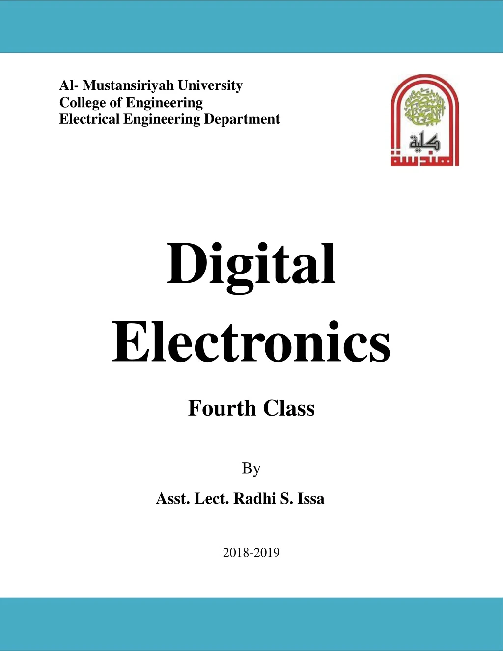
Al- Mustansiriyah University College of Engineering Electrical Engineering Department. Digital Elect r onics Fourth Class. By Asst . Lect. Radhi S. Issa 201 8 -201 9. Syllabus: Timing Circuits. The 555 Timer.

E N D
Al- Mustansiriyah University College of Engineering Electrical EngineeringDepartment Digital Electronics FourthClass By Asst. Lect. Radhi S.Issa 2018-2019
Syllabus: Timing Circuits. The 555Timer. Shift Registers, Sequence Generator and Counters. 4- Design and Analysis of Finite StateMachine. 5- Digital to Analog Converters (DAC) & Analog to Digital (ADC). 6- Programmable Logic Devices. Logic Families. Semiconductor Memories. ــــــــــــــــــــــــــــــــــــــــــــــــــــــــــــــــــــــــــــــــــــــــــــــــــــــــــــــــــــــــــــــــــــــــــــــــ References: 1-Thomas L. Floyd, "Digital Fundamentals" 2009. 2- C.H. Roth, "Fundamental of LogicDesign". 3- M. Morris Mano and Michael D. Ciletti, "DIGITAL DESIGN". 4- Douglas lewin, " Design of logic systems". 5- M. Morris Mano and C.R. Kime, "Logic and Computers Design Fundamentals". 1
TIMER CIRCUITS The 555 Timer The 555 timer is a versatile and widely used device because it can be configured in two different modes either as a Monostable Multivibrator (One-Shot) or as an Astable Multivibrator (Oscillator). An Astable Multivibrator has no stable states and therefore changes back and forth (Oscillates) between two unstable states without any externaltriggering. Basic Operation A functional diagram showing the internal components of a 555 timer is given in Fig.(1.1). VCC (8) The555 Timer R 5k (6) Threshold Control voltage ComparatorA + (5) - Latch R (3) R Q Output Output buffer S 5k + (2) - Trigger ComparatorB (7) Discharge Q1 R Discharge transistor 5k (1) (4) GND Reset Fig. (1.1): Internal functional diagram of a 555timer (Pin numbers are inparentheses) 3
The comparators are device whose outputs are HIGH when the voltage on the positive (+) input is greater than the voltage on the negative (-) input and LOW when the (-) input voltage is greater than the (+) input voltage. The voltage divider consistingofthree(5-kΩ)resistorsprovidesatriggerlevelof1 3VCCanda threshold level of 2 3VCC . The control voltage input (pin 5) can be used to externally adjust the trigger and threshold levels to other values if necessary. When the normally HIGH trigger input momentarily goes below 1 3VCC , the output of comparator B switches from LOW to HIGH and set the S-R latch, causing the output (pin 3) to go HIGH and turning the discharge transistor Q1 off. The output will stay HIGH until the normally LOW threshold input goes above 2 3VCC and causes the output of comparator A to switch from LOW to HIGH. This resets the latch, causing the output to go back LOW and turning the discharge transistor on. The external reset input can be used to reset the latch independent of the threshold circuit. The trigger and threshold input (pin 2 and 6) are controlled by external components connected to produce either Monostable or Astableaction. Monostable (One-Shot)Operation: An external resistor and capacitor connected as shown in Fig. (1.2) are used to set up the 555 timer as a non- retriggerable one-shot. The pulse width of the output is determined by the values of R1 and C1. The control voltage input is not used and is connected to a decoupling capacitor C2 to prevent noise from affecting the trigger and thresholdlevels. The three equal resistance R establish the reference voltages VA and VB for comparators A and B respectively as VA= 2Vcc/3, VB= Vcc/3. Before a trigger pulse is applied, the SR latch is reset with Q=V(0), so the output is LOW, thedischarge transistor Q1 is on, keeping C1 discharge and the threshold voltage Vx=0, asshown inFig.(1.3a). When a negative-going trigger pulse is applied the output goes HIGH and the discharge transistor turns off, allowing capacitor C1 to begin chargingthrough R1
4 as shown in Fig. (1.3b). When C1 charges to 1 3VCC , the output goes back LOW and Q1 turn on immediately, discharging C1 as shown in Fig. (1.3c). As you can see, the charging rate of C1 determines how long the output isHIGH. The pulse width T1 is determined by the time required for thecapacitance voltage Vx to charge VAfor: So The thresholdvoltage: Vx = Vcc- (Vcc- V(0))𝒆−𝒕/𝐑𝟏𝐂𝟏 0 ≤ τ ≤T1 at t=T1 when Vx(T1)= VA=2Vcc/3 T1=R1C1ln𝐕𝐜𝐜−𝐕(𝟎) , V(0) ≈0 𝐕𝐜𝐜/𝟑 T1= R1C1 ln 3 = 1.1R1C1 T1= 1.1R1C1 …(1) +VCC (4) (8) R1 RESET DISCH VCC (7) (6) The 555 Timer (3) OUT THRESH TRIG (2) (5) CONT C2 C1 0.01F GND (decouplingoptional) (1) Fig.(1.2): The 555 timer connected as a oneshot.
VCC 5 Fig. (1.3a): Prior fortriggering. (8) The555 Timer R R1 5k A + LOW _ (6) (5) R HIGH (3) LOW R Q S Output 5k B + HIGH (2) - LOW Trigger (7) Q1 R ON 0V C1 5k (1) (4) VCC Fig. (1.3b): Whentriggered. (8) The555 Timer R R1 (6) 5k A + LOW - (5) R t0 t0 (3) VC1 R Q Output S 0 5k B + t0 (2) - (7) Charging Q1 R OFF C1 5k (1) (4)
VCC 6 Fig. (1.3c): At end of charginginterval. (8) The555 Timer R R1 (6) 5k A + t1 _ 1.1R1C1 (5) t0 t1 t0 Output R t1 (3) 2/3VCC VC1 0 R Q S +B 5k t0 t1 (2) _ LOW HIGH (7) Discharging Q1 R ON C1 att1 5k (1) (4) EXAMPLE (1): What is the output pulse width for a 555 Monostable circuit with R1=2.2 kand C1=0.01F? Solution: From equation (1) the pulse widthis tw=1.1 R1.C1=1.1*(2.2 kFs. Homework For C1=0.01µF, determine the value of R1 for a pulse width of 1ms.
7 Astable (Free Running)Operation: A 555 timer is connected to operate as an Astable Multivibrator, It is a non- sinusoidal Oscillator as shown in Fig. (1.4). Notice that the threshold input (THRESH) is now connected to the trigger input (TRIG). The external components R1, R2, and C1 from the timing network sets the frequency of oscillation. The(0.01 µF) capacitor C2 connected to the control (CONT) input is strictly used for decoupling and has no effect on the operation, in some cases it can be leftoff. Initially, when the power is turned on, the capacitor C1 is uncharged and thus the trigger voltage (pin 2) is at (0 V). This causes the output of comparator B to be HIGH and the output of comparator A to be LOW, forcing the output of the latch and thus the base of Q1 to be LOW and keeping the transistor off. Then C1 begins charging through R1 and R2 as indicated in Fig. (5). When the capacitor voltage reaches1 3VCC,comparatorBswitchestoitsLOWoutputstate,andwhenthe capacitor voltage reaches 2 3VCC , comparator A switches to its HIGH output state, this resets the latch, causing the base of Q1 to go HIGH and turning on the transistor.ThesequencewillcreateadischargepathforthecapacitorthroughR2 and the transistor, as indicated. The capacitor now begins to discharge, causing comparatorAtogoLOW.Atthepointwherethecapacitordischargesdownto 1 3VCC,comparatorBswitchesHIGH,thiswillsetthelatch,makingthebaseof Q1 to be LOW and turning off the transistor. Another charging cycle begins, and the entire process repeats. The result is a rectangular wave output whose duty cycle depends on the values of R1 and R2. The frequency of oscillation is given by the formula: 1.44 f . ( R1 2R2)C1 …(2)
+VCC 8 (4) (8) R1 RESET DISCH VCC (7) The 555 Timer R2 (6) (3) OUT THRESH (2) (5) CONT TRIG C2 C1 0.01F GND (decouplingoptional) (1) Fig. (1.4): The 555 timer connected as an AstableMultivibrator +VCC (8) The555 Timer R 5k A + _ (6) (5) R1 R (3) R Q Vout Charging S 5k B + (2) 2 1 2 1 _ (7) Q1 2 1 2 1 On OffOn R R2 5k 222+ 2/3VCC 1/3VCC _C1 (1) (4) Discharging 1 1 +VCC Fig. (1.5): Operation of 555 timer in the Astable mode 9
By selecting R1 and R2, the duty cycle of the output can be adjusted. Since C1 charges through R1+R2 and discharges only through R2, duty cycles approaching a minimum of 50 percent can be achieved if R2>>R1 so that the charging and discharging times are approximately equal. An expression for the duty cycle is developed as follows. The time that the output is HIGH (tH) is how long it takes C1 to charge from 1 3VCC to 2 3VCC . It is expressedas, tH 0.7( R1 R2)C1. …(3) The time that the output is LOW (tL) is how long it takes C1 to dischargefrom 2 3VCC to 1 3VCC . It is expressedas …(4) tL 0.7R2C1. The period, T, of the output waveform is the sum of tH andtL. T tH tL 0.7( R1 2R2 )C1. This is the reciprocal of (f) in equation (2). Finally, the duty cycleis …(5) tH Duty Cycle tH . T tH tL …(6) RR Duty Cycle1 2100%. R12R2 To obtain a duty cycles of less than 50 percent, the circuit in Fig. (1.4) can be modified so that C1 charges through only R1 and discharges through R2. This is achieved with a diode D1 placed as shown in Fig. (1.6). The duty cycle can be made less than 50 percent by making R1 less than R2. Under this expression for the dutycycle: R1 Duty Cycle100%. R R 1 2 10
+VCC (8) (3) OUT (5) CONT C2 0.01F C1 GND (1) Fig.(1.6): The addition of diode D1 allows the duty cycle of the output to be adjusted to less than 50 percent by makingR1<R2 EXAMPLE (2): A 555 timer configured to run in the Astable mode (Oscillator) is shown in figure below. Determine the frequency of the output and the duty cycl+e5..5V (4) (8) R1 RESET VCC DISCH 2.2k (7) R2 4.7k The 555 (6) (3) OUT THRESH (2) C1 (5) TRIG TimerCONT C2 0.01F GND 0.022F (1) 11
Solution: Use Equations (2 and6). 1.441.44 f 5.64kHz ( R1 2R2)C1 ( 2.2k9.4k)0.022F R1 R2 2.2k4.7k Duty cycle100%100% 59.5%. R 2R 2.2k9.4k 1 2 Homework Determine the duty cycle in figure above if a diode is connected across R2 as indicated in Fig. (6). 12
EXAMPLE(3): Determine the output frequency and duty cycle of the 555oscillator. 13
EXAMPLE (4): Determine the output pulse width shown in figurebelow: 14