Download
1 / 12
120 likes | 275 Views
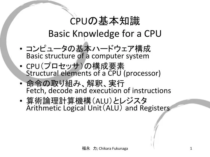
CPU の基本 知識 Basic Knowledge for a CPU. コンピュータの基本ハードウェア構成 Basic structure of a computer system CPU (プロセッサ)の構成要素 Structural elements of a CPU (processor) 命令の取り組み、解釈、実行 Fetch, decode and execution of instructions 算術論理計算機構( ALU )とレジスタ Arithmetic Logical Unit ( ALU ) and Registers.

E N D
CPUの基本知識Basic Knowledgefor aCPU • コンピュータの基本ハードウェア構成Basic structure of a computer system • CPU(プロセッサ)の構成要素Structural elements of a CPU (processor) • 命令の取り組み、解釈、実行Fetch, decode and execution of instructions • 算術論理計算機構(ALU)とレジスタArithmetic Logical Unit(ALU) and Registers 福永 力; Chikara Fukunaga
コンピュータの基本ハードウェア構成Basic hardware structure of a computer • 中央処理装置(CPU)Central Processor Unit(CPU) • メモリMemory (2n Byte Space=Address n bit) • Space n=8/256, 16/64k, 32/4GB • プログラム内蔵方式では必須Essential for Program Storage • ROM: Read Only Memory • RAM: Read Access Memory • 入出力装置I/O Interface • Parallel: PCI … • Serial: USB, Video-graphic, Ethernet, Firewire … 福永 力; Chikara Fukunaga
プロセッサの構成要素Principal structure of a CPU • Processor = CPU in a single chip • Microprocessor (Intel) = Processor • Microcomputer = Processor+Memeory+I/O I/F 福永 力; Chikara Fukunaga
命令の取り組みと実行Fetch,decode & execution of instructions • プログラム(メモリ内収録)から命令(Instruction)の取り組み(Fetch) • Instructionの解析(Decode) • Instructionの実行(Execution) 福永 力; Chikara Fukunaga
命令形式例Examples of instruction formats 福永 力; Chikara Fukunaga
演算機とレジスターArithmatic Logical Unit (ALU) & Registers • CPUに用いられるさまざまなレジスタの例Examples of Various registers used in a CPU • 汎用(浮動小数点演算)レジスタGeneral Purpose Registers: GPR0-31 (32 32-bit registers)Floating Point Registers: FPR0-31 (32 64-bit registers) • 状態保存, 例外検知レジスタ:Condition Register: CR, FPCReXceptional Execution Reg.: XER • プログラムカウンタ:Program Counter: PC • powerPC4の例Example of powerPC4 • Instr. rD,rS,rB(rD ← rS・rB) (・= any binary calcul.) 福永 力; Chikara Fukunaga
CPU、Cacheとメモリのつなぎの変遷Development of CPU, cache and Memory connection 福永 力; Chikara Fukunaga
最初の1 chip processor Intel 4004First single chip processor Intel 4004 • 日本のビジコン社電卓用に開発されたDeveloped for a electric calculator of Busicom ltd. Japan • 同社は小型高速プリンター付電卓の開発を目論むThe company wants to develop small calculator with a printer • インテルに制御用LSIの開発以来The company asked Intel to develop several LSIsfor calculator control • インテル、マイクロコンピュータセットの提案Intel proposed a microcomputer set for this control (CPU, ROM, RAM, Shift registers) • 1969年4月ビジコン社、11月商品として発売Apr.,1971 completed, Nov. ,1971 released 福永 力; Chikara Fukunaga
4004の概要Overview of 4004 • 4 bit CPU w/ 46 instructions • Clock 750kHz • 命令(Instructions) with 1 word (8bit) 8 clock (3 clock for 12-bit address, 2 clock for 8-bit instruction, 3 clock for execution) 2 word (16bit) 16 clock (8clock×2word) • Address space 4kB (12bit) for ROM/RAM • 16 4-bit/8 8-bit general purpose registers • Address stack for subroutine calls (depth 4) • 現代のプロセッサとほぼ同じ内部構造(Almost similar architecture with amodern processor chip) 福永 力; Chikara Fukunaga
その後の発展(1)After 4004 • 1971-1973(First generation) • Intel 4004(4bit) • Intel 8008(8bit)文字列操作 for alphanumeric handling • 4-8bit • プログラム Program with 機械語 machine language、アセンブリassembly • pMOSトランジスタ Transistor(O(1k)) 福永 力; Chikara Fukunaga
その後の発展(2)after 8008 • 1974-1976(第2世代;2nd generation) • 8-bit Intel 8080、Motorola 6800 • プログラム program with assembly、compiler(assembler) • nMOSトランジスタ Transistor • (Development of )DRAMの発展(4kbit) • (Floppy based) ディスクオペレーティングシステムDisk Operating System DOS • nMOSトランジスタ Transistor(O(3-10k)) • Zilog Z80(~8080) with new nMOS technology 福永 力; Chikara Fukunaga
その後の発展(3)After Z80 • 1977-1986(第3世代;3rd generation) • 16-bit Intel 8086、80286、Z8000、M680x0 • プログラミングAssembly(assembler)、C、Basic • 8086→MS/DOS、68000→Mac/Apple • Network、 Graphics • HMOS(High performance nMOS)トランジスタTransistor(O(100k)) • CMOS process (1980以降) • 1987(第4世代;4th generation)32-bit • Intel 80386、Pentium、powerPC、RISC 福永 力; Chikara Fukunaga