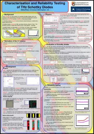
Download
1 / 8
80 likes | 322 Views
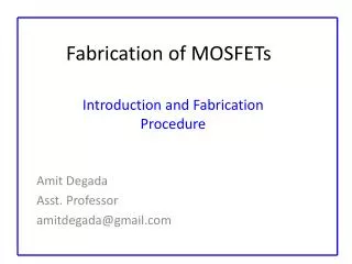
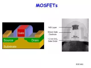
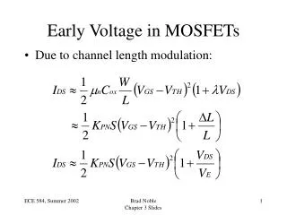
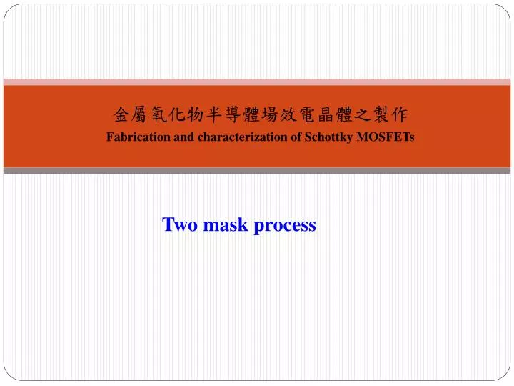
金屬氧化物半導體場效電晶體之製作 Fabrication and characterization of Schottky MOSFETs. Two mask process. The goal of this class is to make a Schottky MOSFETs. Gate. Source. Drain. Gate. Metal. SiO 2. Source. Drain. SiO 2. SiO 2. Metal. Metal. Si. Cross section. Top view. 1. 清洗樣品. acetone. BHF.

E N D
金屬氧化物半導體場效電晶體之製作 Fabrication and characterization of Schottky MOSFETs Two mask process
The goal of this class is to make a Schottky MOSFETs Gate Source Drain Gate Metal SiO2 Source Drain SiO2 SiO2 Metal Metal Si Cross section Top view
1.清洗樣品 acetone BHF methanol 1. 將 sample 放入裝有丙酮的燒杯裡,使用超音波震洗機 震洗 3 min。 2. 使用 甲醇 洗去sample 的丙酮 ,將樣品放入裝有甲醇的燒杯裡,使用 超音波震洗機 震洗 3 min。 3. 使用 DI water (去離子水) , 沖洗 sample 1min。 4. 使用 BHF 蝕刻 native oxide 5. 使用 氮氣槍 仔細吹乾 sample 表面。
2.定義S/D圖形 目的: 利用曝光顯影的技術,將需要鍍S/D金屬的區域定義出來。 1. 塗佈光阻 (A) 將 sample 放置於 塗佈機上, 旋轉測試 1000 轉 10 sec,4000 轉 40 sec。 (B) 測試完畢後,sample 滴滿光阻,啟動。 (C) 拿取 sample。 2. 曝前烘烤 (軟烤) 放加熱板(hot plate)上95oC,2 min。 3. 曝光 (A) 放置光罩 (鍍金屬的面朝sample) (B) 放置 sample , 曝光 18 sec。 4. 烘烤+曝光 (正光阻轉換成負光阻) 將 sample放加熱板(hot plate)上115oC,2min。 曝光 50 sec 5. 顯影 將 sample 置入顯影液,顯影 30 sec,過DI 15sec。 6. 硬烤 放加熱板(hot plate)上 110oC, 3 min。
3.鍍S/D金屬 • 鍍金屬,參考實驗二 • 2. Lift off:將光阻及光阻上之金屬去除,留下S/D金屬。 • (A) 將sample放入裝有丙酮的燒杯裡,使用超音波震洗機 震洗 1 min。 • (B) 使用甲醇洗去sample的丙酮 ,將樣品放入裝有甲醇的燒杯裡, • 超音波震洗機 震洗 1 min。 • (C) 使用 DI water (去氧離子水),沖洗 sample 1min。 • (D) 使用 氮氣槍 仔細吹乾 sample 表面的水。
4.沉積閘極氧化層 使用PECVD沉積SiO2當閘極氧化層 5. 定義閘極圖形 目的: 利用曝光顯影的技術 , 將需要鍍閘極金屬的區域定義出來。 參考步驟二、定義S/D圖形 6. 鍍閘極金屬 參考步驟三、鍍S/D金屬 7. 蝕刻S/D上之SiO2 利用RIE或BHF蝕刻SiO2 8. 鍍背電極
結報問題 1.Id-Vg & Id-Vd 2.Vt、on/off、SS、DIBL 3. What is GIDL (Gate Induced Drain Leakage)