Download
1 / 79
790 likes | 906 Views
Chapter 21 Cache. Reference: [1] David A. Patterson and John L. Hennessy, Computer Organization & Design

E N D
Chapter 21 Cache Reference: [1] David A. Patterson and John L. Hennessy, Computer Organization & Design [2] Bruce Jacob, Spencer W. Ng, David T. Wang, Memory Systems Cache, DRAM, Disk [3] Multiprocessor: Snooping Protocol,www.cs.ucr.edu/~bhuyan/CS213/2004/LECTURE8.ppt [4] EEL 5708 High Performance Computer Architecture, Cache Coherency and Snooping Protocol, classes.cecs.ucf.edu/eel5708/ejnioui/mem_hierarchy.ppt [5] Willian Stallings, Computer Organization and Architecture, 7th edition [6] Intel 64 and IA-32 Architectures Software Developer’s Manual, volume 1: Basic Architecture [7] Intel 64 and IA-32 Architectures Optimization Reference Manual Speaker: Lung-Sheng Chien
OutLine • Basic of cache- locality - direct-mapped, fully associative, set associative • Cache coherence • False sharing • Summary
Basic logic gate 1. AND gate a c b 2. OR gate a c b 3. inverter a c d 4. multiplexer a c b
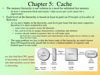
Principle of locality • Temporal locality (locality in time): if an item is referenced, it will tend to be referenced again soon. • Spatial locality (locality in space): if an item is referenced, items whose addresses are close by will tend to be referenced soon. • Algorithmic locality: traverse linked-list (may not be spatial locality) for-loop is temporal locality array is spatial locality Observation: temporal locality means that we don’t put all program into memory whereas spatial locality means that we don’t put all data into memory, hence we have “Memory Hierarchy”
Memory Hierarchy Speed CPU Size Cost ($/bit) smallest highest fastest L1 cache on chip L2 cache on chip Main memory biggest lowest slowest Definition: If the data requested by processor appears in upper level, then this is called a “hit” , otherwise, we call “miss”. Conventionally speaking, cache hit or cache miss Definition: “Hit time” is the time to access upper level memory, including time needed to determine whether the access is a hit or a miss. Definition: “miss penalty” is the time to replace a block in upper level with corresponding block from lower level, plus the time to deliver this block to processor.
Basic of cache [1] Direct-mapped cache: each memory location is mapped to exactly one location in cache Mapping rule: (block address) modulo (number of cache block in the cache) • Cache: a safe place for hiding or storing things Main memory 0b00000 0b00001 0b00010 cache 0b00011 0b00100 0b000 0b00101 0b001 0b00110 0b010 0b00111 0b011 0b01000 0b100 0b01001 0b101 0b01010 0b110 0b01011 0b111 0b01100 0b01101 0b01110 0b01111 0b10000 0b10001 Observation: we only use 3 least significant bits to determine address.
Basic of cache [2] Question 1: size of basic block of cache (also called cache line size) Question 2: if data is in cache, how to know whether a requested word is in the cache or not? Question 3: if data is not in cache, how do we know? Address (showing bit position) 31 30 … 13 12 11 … 2 0 1 Byte offset Basic block is a word (4 byte), since each memory address binds a byte, so 4-byte require 2 bits. 20 Tag 10 index Index Valid Tag Data 0 Use 10 bits to index address in cache, total number of block in the cache is 1024 1 Data 2 ….. …… …… Tag contains the address information required to identify whether a word in the cache corresponding to the requested word. 1021 1022 1023 20 32 Valid bit: indicates whether an entry contains a valid address. = Hit
Basic of cache [3] Configuration: Basic block of cache is word (4-byte), and cache has 4 blocks Most significant bit 5 4 3 2 1 0 Least significant bit 1 0 0 1 1 1 word Index of the cache tag 0b100000 0b000000 0b010000 33 1 17 0b100001 0b000001 0b010001 34 2 cache 18 0b100010 0b000010 0b010010 valid 35 3 19 0b100011 0b000011 tag 0b010011 36 4 20 data 0b100100 0b000100 0b010100 37 5 21 index 0b100101 0b000101 0b010101 38 6 22 0b100110 0b000110 0b00 0b010110 39 7 1 00 4 3 2 1 23 0b100111 0b000111 0b01 0b010111 40 8 1 00 8 7 6 5 24 0b101000 0b001000 0b10 0b011000 41 9 1 00 12 11 10 9 25 0b101001 0b001001 0b11 0b011001 42 10 1 00 16 15 14 13 26 0b101010 0b001010 0b011010 43 11 27 0b101011 0b001011 0b011011 44 12 28 word (4-byte) 0b101100 0b001100 0b011100 45 13 29 0b101101 0b001101 0b011101 46 14 30 0b101110 0b001110 0b011110 47 15 31 0b101111 0b001111 0b011111 48 16 32
Basic of cache [4] Question 4: is data with address 0b100111 in the cache? Index of the cache tag word Most significant bit 5 4 3 2 1 0 Least significant bit 1 0 0 1 1 1 cache valid tag 2 data 2 index 0b00 1 00 4 3 2 1 0b01 1 00 8 7 6 5 0b10 1 00 12 11 10 9 0b11 1 00 16 15 14 13 word (4-byte) 00 10 = 1 0 miss 0
Example of direct-mapped cache [1] Initial state of cache 1. Access 0b10110 miss miss 2. Access 0b11010 3. Access 0b10110 hit
Example of direct-mapped cache [2] 4. Access 0b10000 miss miss 5. Access 0b00011 6. Access 0b10010 miss
Advantage of spatial locality [1] 64kB cache with a word (4 byte) as block size Address (showing bit position) 31 30 … 17 16 15 … 5 4 3 2 0 1 Byte offset 16 Tag 14 index 16 bits 32 bits Valid Tag Data Data To take advantage of spatial locality, we want to have a cache block that is larger than one word in length, why? 16Kentries When a miss occurs, we will fetch multiple words that are adjacent and carry a high probability of being needed shortly. 16 32 = Hit
Advantage of spatial locality [2] 64kB cache using 4 words (16 byte) blocks 31 30 … 17 16 15 … 6 5 4 3 2 0 1 Byte offset 16 Tag 14 Block offset index 16 bits Data 128 bits Valid Tag Data 4Kentries 32 32 16 32 32 32 = 2 Hit Mux 1. Total number of blocks in cache is 4K, not 16K 2. We need signal block offset (2 bits) to determine which word we need 3. Mapping rule: (block address) modulo (number of cache block in the cache)
Advantage of spatial locality [3] Exercise 1: consider a cache with 64 blocks and a block size of 16 bytes. What block number does byte address 1203 map to (assume 12-bit address)? mask to 16 bytes (a block) 1 Find block address 2 mapping rule: (block address) modulo (number of cache block in the cache) 3 Index of the cache 4-words tag Most significant bit 11 10 9 8 7 6 Least significant bit 5 4 3 2 1 0 0 1 0 0 1 0 1 1 0 0 1 1 data index tag 0 1 2 11 1 01 Mem(4BC) Mem(4B8) Mem(4B4) Mem(4B0)
Advantage of spatial locality [4] miss rate versus block size Exercise 2: take a simple for-loop, discuss lager block size can reduce miss rate Question 5: why does miss rate increase when block size is more than 64 bytes? Question 6: what is trend of mss penalty when block size is getting larger? (miss penalty is determined by the time required to fetch the block from the next lower level of memory hierarchy and load it into the cache. The time to fetch the block includes 1. latency to first word and 2. transfer time for the rest of the block)
Memory system versus cache [1] Assumption : • 1 clock cycle to send the address (Cache DRAM) • 15 clock cycles for each DRAM access initiated • 1 clock cycle to send a word of data (depend on width of the bus) • Cache block is 4-words CPU miss penalty = 1 + 4 x 15 + 4 x 1 = 65 clock cycles Cache send address initiate DRAM 4 times, each time for one word Bus Memory (DRAM) send a word through bus one by one since width of bus is one-word Number of bytes transferred per clock cycle for a single miss = one-word-wide memory organization
Memory system versus cache [2] miss penalty = 1 + 15 + 1 = 17 clock cycles CPU send address initiate DRAM one time and fetch 4 words Multiplexor Cache send 4 words through bus since width of bus is 4-words Bus Memory (DRAM) 4-word-wide memory organization Number of bytes transferred per clock cycle for a single miss = Question 7: what is drawback of wide memory organization ?
Memory system versus cache [3] miss penalty = 1 + 15 + 4x1 = 20 clock cycles CPU send address initiate DRAM one time and fetch 4 words Cache send one words through bus one by one since width of bus is one word. Bus Memory bank 0 Memory bank 2 Memory bank 3 Memory bank 1 interleaved memory organization Number of bytes transferred per clock cycle for a single miss = Question 8: what is difference between wide memory organization and interleaved memory organization ?
Two level decoder of DRAM [3] row access chooses one row and activates corresponding word line 1 contents of all the columns in the active row are stored in a set of latches (page mode) 2 3 column access selects data from the column latches row access uses 11 bits to select a row
Improve cache performance • Reduce miss rate:reduce probability that two different memory blocks will contend for the same cache location. • Reduce miss penalty:add an additional level of hierarchy, say L1 cache, L2 cache and L3 cache. Direct-mapped cache: each memory location is mapped to exactly one location in cache Mapping rule: (block address) modulo (number of cache block in the cache) Fully-associative cache: each block in memory may be associated with any entry in the cache. Mapping rule: exhaust search each entry in cache to find an empty entry set-associative cache Direct-mapped cache Fully-associative cache Index is regular Index is at random
Example of fully-associative cache [1] Initial state of cache 1. Access 0b10110 miss miss 2. Access 0b11010 3. Access 0b10110 hit
Example of fully-associative cache [2] 4. Access 0b10000 miss miss 5. Access 0b00011 6. Access 0b10010 miss
set-associative cache Two-way set associative One-way set associative (direct mapped) Set Tag Data Tag Data Block Tag Data 0 0 1 1 2 2 3 3 four-way set associative 4 5 Set Tag Data Tag Data Tag Data Tag Data 6 0 7 1 eight-way set associative (fully-associative) Tag Data Tag Data Tag Data Tag Data Tag Data Tag Data Tag Data Tag Data A set-associative cache with n locations for a block is called an n-way set-associative cache Mapping rule: (block address) modulo (number of sets in the cache)
Associativity in cache [1] Example: there are three small caches, each consisting of 4 one-word blocks. One cache is fully-associative, a second is two-way set associative and the third is direct mapped. Find the number of misses for each cache organization given the following sequence of block addresses: 0, 8, 0, 6, 8. Two-way set associative Set Tag Data Tag Data One-way set associative (direct mapped) 0 Block Tag Data 1 0 fully-associative 1 Tag Data Tag Data Tag Data Tag Data 2 3 Direct-mapped cache : (block address) modulo (number of block in the cache) 1
Associativity in cache [2] two-way associative cache : (block address) modulo (number of sets in the cache) 2 Replace least recently used block
Associativity in cache [3] Fully associative cache : exhaust search for empty entry 3 Number of Miss : Direct-mapped (5) > two-way associative (4) > fully associative (3) Question 9: what is optimal number of miss in this example? Question 10: How about if we have 8 blocks in the cache? How about 16 blocks in the cache?
Implementation of set-associative cache 31 30 … 11 10 9 8… 2 1 0 22 8 Tag index V Tag Data V Tag Data V Tag Data Index V Tag Data 0 1 2 253 254 255 22 = = = = 32 4-to-1 Mux OR Hit Data The tag of every cache block with appropriate set is checked to see if it matches the block address. In order to speedup comparison, we use 4 comparators to do in parallel
Reduce miss penalty using multi-level caches [1] • Reduce miss rate:reduce probability that two different memory blocks will contend for the same cache location. • Reduce miss penalty:add an additional level o hierarchy, say L1 cache, L2 cache and L3 cache. CPI : average clock cycles per instruction CPU time = instruction count x CPI x clock cycle time 1 R/W 2 miss 3 miss CPU L1 cache L2 cache DRAM 4 R/W 5 R/W 6 R/W
Reduce miss penalty using multi-level caches [2] Example: suppose a processor (clock rate 500MHz) with a base CPI of 1.0, assuming all references hit in the L1 cache. Assume a main memory access time of 200ns, including all the miss handling. Suppose miss rate per instruction at L1 cache is 5%. How much faster will the machine be if we add a L2 cache that has 20 ns access time for either a hit or a miss and is large enough to reduce miss rate to main memory to 2%? 500MHz Miss rate 5 % R/W DRAM CPU L1 cache R/W need time 200ns Hit rate 95 % 500MHz 2ns / clock cycle 1 Miss penalty to main memory = 200ns / 2ns = 100 clock cycles (CPU clock cycle) 2 3 The effective CPI with L1 cache is given by Total CPI = base CPI + memory-stall cycles per instruction = 1.0 + 5% x 100 = 6.0 500MHz Miss rate 5 % Miss rate 2 % R/W L2 cache CPU L1 cache DRAM R/W need time 200ns R/W need time 10ns
Reduce miss penalty using multi-level caches [3] 500MHz Miss rate 5 % Miss rate 2 % R/W L2 cache CPU L1 cache DRAM R/W need time 200ns R/W need time 10ns 4 Miss penalty of L1 cache for an access to L2 cache = 20ns / 2ns = 10 clock cycles 5 L1 cache hit rate 95 % Miss rate 5 % L2 cache hit rate 3 % Miss rate 2 % Total CPI = 1.0 + stalls per instruction due to L1 cache miss and L2 cache hit stalls + stalls per instruction due to L1 cache miss and L2 cache miss = 1+ (%5 - %2) x 10 + 2% x (10 + 100) = 1 + 0.3 + 2.2 = 3.5 The machine with L2 cache is faster by 6.0 / 3.5 = 1.7 6 Remark: L1 cache focus on “hit time” to yield short clock cycle whereas L2 cache focus on “miss rate” to reduce penal of long memory access time.
OutLine • Basic of cache • Cache coherence- simple snooping protocol- MESI • False sharing • Summary
Write policy in the cache • Write-though: the information is written to both the block in cache and block in main memory. • Write-back: information is only written to the block in cache. The modified block is written to main memory only when it is replaced. Advantage of write-back • Individual words can be written by the processor in the cache level, fast! • Multiple writes within a block requires only one write to main memory • When blocks are written back, the system can make effective use of a high bandwidth transfer. disadvantage of write-back • Interaction with other processors when RAW (Read after Write) hazard occurs, say other processor will read the incorrect data in its own cache. Advantage of write-through • Misses are simpler and cheaper because they never require a block in cache to be written to main memory. • Easy to implement than write-back, a write-through cache only needs a write buffer. disadvantage of write-through • Cost since write to main memory is very slow
Consistency management in cache • Keep the cache consistent with itself: avoid two copies of a single item in different places of the cache. • Keep the cache consistent with the backing store (main memory): solve RAW (Read after Write) hazard - write-through policy- write-back policy • Keep the cache consistent with other caches- L1 cache versus L2 cache in the same processor- L1 cache versus L1 cache in different processors- L1 cache versus L2 cache in different processors- L2 cache versus L2 cache in different processorstwo policies: inclusion or exclusion CPU L1 cache on chip Inclusion: L2 cache off chip Main memory
What Does Coherency Mean? • Informally: • “Any read must return the most recent write” • Too strict and too difficult to implement • Better: • “Any write must eventually be seen by a read” • All writes are seen in proper order (“serialization”) • Two rules to ensure this: • “If P writes x and P1 reads it, P’s write will be seen by P1 if the read and write are sufficiently far apart” • Writes to a single location are serialized: seen in one order • Latest write will be seen • Otherwise could see writes in illogical order (could see older value after a newer value)
Potential Hardware Coherency Solutions • Snooping Solution (Snoopy Bus): • Send all requests for data to all processors • Processors snoop to see if they have a copy and respond accordingly • Requires broadcast, since caching information is at processors • Works well with bus (natural broadcast medium) • Dominates for small scale machines (most of the market) • Directory-Based Schemes • Keep track of what is being shared in one centralized place • Distributed memory => distributed directory for scalability(avoids bottlenecks) • Send point-to-point requests to processors via network • Scales better than Snooping • Actually existed BEFORE Snooping-based schemes
Cache coherency in multi-processor: snooping protocol [1] All cache controllers monitor (snoop) on the bus to determine whether or not they have a copy of the shared block • Maintaining coherency has two components: read and write- read: not a problem with multiple copies- write: a processor must have exclusive access to write a word, so all processors must get new values after a write, say we must avoid RAW hazard • The consequence of a write to shared data is either - to invalidate all other copies or- to update the shared copies with the value being written Snoop tag is used to handle snoop requests
Cache coherency in multi-processor: snooping protocol [2] Read hit : normal read Read miss : all caches check to see if they have a copy of the requested block and then supply data to the cache that missed write miss / hit : all caches check to see if they have a copy of the requested block and then either invalidating or updating their copy Snooping protocols are of two types • Write-invalidate: similar to write-back policy (commercial used)- multiple readers, single writer- write to shared data: an invalidate signal is sent to all caches which snoop and invalidate any copies.- Read miss: (1) write-through: memory is always up-to-date (2) write-back: snoop in caches to find most recent copy • Write-update: similar to write-through - writing processor broadcasts the new data over the bus, then all copies are updated with the new value. This would consume much bus bandwidth. Write-invalidation protocol based on write-back policy. Each cache block has three states • Shared (Read only): this cache block is clean in all caches and up-to-date in memory, multiple read is allowed. • Exclusive (Read/Write): this cache block is dirty in exactly one cache. • Invalid: this cache block does not have valid data
Simple snooping protocol [1] color: bus signal, including read miss, write miss color: CPU write write miss CPU read hit color: CPU read Invalid shared (Read only) CPU read, place read miss on bus CPU read miss, place read miss on bus CPU write, place write miss on bus write miss write-back block CPU read miss, Write-back data place read miss on bus CPU write,place write miss on bus exclusive (Read/Write) CPU read hit CPU write hit read miss, Write-back data CPU write miss, write-back data, place write miss on bus
Simple snooping protocol [2] Cache coherence mechanism receives requests from both the processor and the bus and responds to these based on the type of request, state of cache block and hit/miss
Example of state sequence [1] Processor 1 Processor 2 Memory Bus • Assumption • Initial cache state is invalid • A1 and A2 map to same cache blockbut A1 is not A2 P1 P2 P1 P2 Invalid Invalid bus
Example of state sequence [2] P2 P1 CPU read hit Invalid write miss Invalid shared CPU read, put read miss on bus Write miss signal on bus does not affect P2 CPU write, put write miss on bus write miss write-back block read miss, write-back data P1 P2 CPU write, put write miss on bus exclusive bus write miss CPU read hit CPU write hit
Example of state sequence [3] P2 P1 CPU read hit Invalid write miss Invalid shared CPU read, put read miss on bus CPU write, put write miss on bus P1 P2 write miss write-back block read miss, write-back data CPU write, put write miss on bus exclusive bus CPU read hit CPU write hit
Example of state sequence [3] P1 P2 CPU read hit exclusive write miss Invalid shared CPU read, put read miss on bus P1 P2 CPU write, put write miss on bus write miss write-back block read miss, write-back data bus read miss CPU write, put write miss on bus exclusive P2 has no A1, so it issues “read miss” signal to P1, then P1 can reply its data to P2 CPU read hit CPU write hit
Example of state sequence [4] P2 P1 CPU read hit shared write miss Invalid shared CPU read, put read miss on bus P1 P2 CPU write, put write miss on bus write miss write-back block read miss, write-back data write-back bus (A1, 10) CPU write, put write miss on bus exclusive P1 write (A1,10) back to DRAM DRAM CPU read hit CPU write hit
Example of state sequence [5] P1 P2 P1 P2 shared shared bus (A1, 10) P1 and P2 are all in state shared, this means that (A1, 10) is shared by two processors and both processors can read (A1,10) at the same time from their own cache without any communication.
Example of state sequence [6] P1 P2 CPU read hit write miss shared Invalid shared CPU read, put read miss on bus P1 P2 CPU write, put write miss on bus write miss write-back block read miss, write-back data bus CPU write, put write miss on bus Write-miss exclusive P2 issues signal “write-miss” to P1, then P1 knows that (A1, 10) is not valid. Then P2 update value of A1 to 20. CPU read hit CPU write hit
Example of state sequence [7] P2 P1 CPU read hit write miss exclusive Invalid shared CPU read, put read miss on bus P1 P2 CPU write, put write miss on bus write miss write-back block read miss, write-back data Write-miss bus CPU write, put write miss on bus exclusive P1 set (A1,10) as invalid, then this data cannot be used any more CPU read hit CPU write hit
Example of state sequence [8] P2 P1 CPU read hit write miss exclusive Invalid shared CPU read, put read miss on bus P1 P2 CPU write, put write miss on bus write miss write-back block read miss, write-back data Write-miss bus CPU write, put write miss on bus exclusive P1 set (A1,10) as invalid, then this data cannot be used any more CPU read hit CPU write hit
Example of state sequence [9] P2 P1 CPU read hit exclusive write miss Invalid shared CPU read, put read miss on bus P1 P2 CPU write, put write miss on bus write miss write-back block read miss, write-back data bus Write-miss CPU write, put write miss on bus exclusive P1 issues signal “write-miss” to P2, then P2 knows that (A1, 20) is not valid. Then P2 must write (A1,20) back to DRAM and then reset cache block to (A2,40) CPU read hit CPU write hit
Example of state sequence [10] P1 P2 CPU read hit exclusive write miss Invalid shared CPU read, put read miss on bus P1 P2 CPU write, put write miss on bus write miss write-back block read miss, write-back data Write-back bus CPU write, put write miss on bus exclusive (A1, 20) DRAM CPU read hit CPU write hit