Download
1 / 65
660 likes | 923 Views
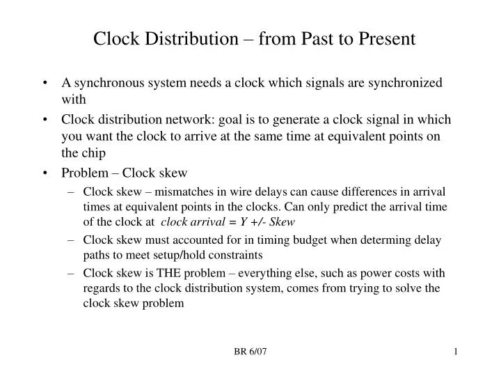
Clock Distribution – from Past to Present. A synchronous system needs a clock which signals are synchronized with Clock distribution network: goal is to generate a clock signal in which you want the clock to arrive at the same time at equivalent points on the chip Problem – Clock skew

E N D
Clock Distribution – from Past to Present • A synchronous system needs a clock which signals are synchronized with • Clock distribution network: goal is to generate a clock signal in which you want the clock to arrive at the same time at equivalent points on the chip • Problem – Clock skew • Clock skew – mismatches in wire delays can cause differences in arrival times at equivalent points in the clocks. Can only predict the arrival time of the clock at clock arrival = Y +/- Skew • Clock skew must accounted for in timing budget when determing delay paths to meet setup/hold constraints • Clock skew is THE problem – everything else, such as power costs with regards to the clock distribution system, comes from trying to solve the clock skew problem BR 6/07
Clock Distribution clk 100 ps 100 ps want clk to arrive at same time at equivalent parts of chip 0 ps reference point 100 ps 100 ps BR 6/07
Clock Distribution (cont) clk 100 ps 100 ps Data if clock arrival is known, can accurately compute delay constraints when sending data from one register to another 0 ps reference point 100 ps 100 ps BR 6/07
Clocking Regions skew to neighboring region: 11 ps local skew: 6 ps local skew: 6 ps clk 98 ps 102 ps 99 ps 92 ps 96 ps 103 ps 97 ps 93 ps 0 ps reference point 100 ps 100 ps Chip is divided into regions, the further a signal has to travel, the larger the skew budget BR 6/07
Skew: Flip-Flops Skew adds to both setup and hold when calculating constraints Source: David Harrison BR 6/07
Clock Distribution Evolution • Alpha 21064 (1993, 750 nm), 150-200 MHz: Global Clock/1 driver/gridded clock, 180 ps clock skew • Alpha 21164 (1995, 500 nm), 300 Mhz –Global Clock, 2 drivers, gridded clock, 80 ps clock skew, • Alpha 21264 (1997/ 350 nm) 500-600 MHz, Clock distribution network – global/local/conditional clocks – deskew by delay insertion, gridded global clock, 65 ps clock skew • IA-64 Gen1 (2000/180 nm) 800 MHz, H-tree global clock, active de-skew (distributed PLLs), 28 ps skew • IA-64 Gen2 (2002/180 nm) 1 GHz, H-tree global clock, regional clocks, NO active deskew, 62 ps skew • IA-64 Gen3 (2003/130 nm) 1.5 GHz, H-tree global clock, regional clocks, fuse-based deskew, 7 ps (scan based) to 24 ps (fuse based) BR 6/07
Clock Distribution Evolution (cont) • IA-64 Dual-core (2004/90 nm) 2.5 GHz (Montecito), H-tree and balanced binary-tree routing, regional clocks, active regional deskew, 10 ps skew • Xeon Dual-core (2006/65 nm) 3.4 GHz (Tulsa) – two different clock systems • Core clocks (clocks for processor cores) uses same core clock scheme as used in Xeon Single Core (2003,/90 nm). This clock scheme was designed to scale up to 6 GHz, and used a H-tree distributed clock with shorted nodes that had produced less than 10 ps skew. No active de-skew or fuse-based de-skew. • Un-core clock (everything outside the core) – Cache, bus logic, etc. Large area prevented use of gridded clock (power restriction), used a clock tree (9 vertical, 2 horizontal) with fuse-based deskew at root of each vertical spine. Achieved less than 11 ps skew. BR 6/07
Definition: Gridded Clock In early clock distribution systems, large drivers + metal clock grid used for clock distribution. Subsystems just tapped into the clock grid for connectivity – easy to do, but takes a lot of power, chews up routing resources (grid density is exaggerated in this picture, there is a lot more white space than is shown BR 6/07
Alpha 21064 Die Photo (1993) Single Clock driver, 2 transistors for buffer visible to naked eye Clocking scheme was 2 phase, single wire. Clock load was 3.5 nF Gate length of final driver was 35 cm (not a misprint, used serpentine layout to get this gate length). BR 6/07
21064 Clock Skew Distribution Max clock skew approx. 180 ps (3.6% of 5 ns clock period) – 1 gate delay about 300 ps, so clock skew about 50% of a gate delay. Note the skew is smallest closest to center of chip where driver is located. BR 6/07
Thermal Image of 20164 76C at center of chip 46C at edges of chip 30C thermal gradient across chip!! BR 6/07
21164 Clock Distribution (1995) Goal of 21164 Clock distribution was to reduce skew by 30% and reduce the thermal gradient. A predriver was centered between two main clock drivers Predriver Clock skew was reduced by factor of 2, and thermal gradient was reduced. Main clock drivers BR 6/07
Max clock skew approx. 80 ps (2.4% of 3.3 ns clock period) – 1 gate delay about 240 ps, so clock skew about 1/3 of a gate delay. Clock skew lowest near two main clock drivers. BR 6/07
Aside: Why a Gridded Clock? • Both 21064, 21164 used a single global clk distributed by a metal clock grid. • Skew is largely determined by grid interconnect density and is insensitive to gate load placement • Why? Because capacitance of grid wiring dominates the gate loads connected to it. • Universal availability of clock signals • Design teams can proceed in parallel since clock constraints well known • Good process-variation tolerance • The disadvantage is the extra capacitance of the grid • Power-performance tradeoff is determined by choice of skew target, which establishes the needed grid density, which determines the clock driver size. BR 6/07
21264 Clock Distribution (1997) • 21264 clocking fundamentally different from previous Alphas because it supported a hierarchy of clocks • Still had a GCLK (global Clk) grid, but conditional and local clocks had several buffer stages after GCLK • Conditional clocks used to save power • Clocks gated to functional units in design • If not executing a floating point instruction, then stop the clock to the floating point unit to save power! • State elements and clocking points were 0 to 8 gates past Gclk • Six major regional clocks two gain stages past GCLK with grids juxaposed with GCLK, but shielded from it. • Major clocks drive local clocks and conditional clocks • Goals were to improve performance, reduce power. BR 6/07
Clock Hierarchy of 21264 BR 6/07
21264 Global Clock Distribution Window pane arrangement - same skew to all ‘panes’ . Note redudant drive to clock nets BR 6/07
Phased Lock Loops (PLLs) • PLLs and Delay Locked Loops (DLLs) are used to perform clock multiplication of an off-chip clock • PLLs/DLLs used to align clock edges of original clock with multiplied clocks • PLLs are analog circuits that use a charge pump and a voltage controlled oscillator (VCO) to perform phase alignment • Alpha 21264 PLL used a separate, regulated 3.3 V supply and was located in the corner of the chip to minimize noise impact • Section 9.5.2 of Rabaey text has a block diagram of a PLL • All high performance CPUs and most ASICs now include a PLL for internal clock generation BR 6/07
Global clock grid. Uses 3% of M3/M4 routing layers (lines in picture are misleadingly thick). BR 6/07
All GCLK lines are laterally shielded by Vss/Vdd signal GCLK signal Vdd Vss Lateral shielding via Vss/Vdd prevents clock noise from coupling into signal lines. Clock wires and lateral shields were manually placed BR 6/07
Simulated worst case GCLK skew was 72 ps . Skew on M1, M2 was less than 10 ps. Measured worst case GCLK skew via ebeam tester was 65 ps BR 6/07
Major clocks are two inversions past GCLK Major clocks saved power over a single global clocks because they service a lighter load and distribution area is smaller – both of these means smaller drivers are needed. Gclk+Major clocks used 24 W @ 2.2 V, 600 Mhz. It is estimated that at least 40W would have been required if only global clocks were used. 10%-90% rise/fall times were targeted at < 320 ps. BR 6/07
Major Clock grids. Densest major clock grids used up to 6% of M3/M4 routing. White areas are serviced by local clocks, local clocks also present in major clock grids. Major clocks also laterally shielded. BR 6/07
Local, Conditional Clocks • Local clocks generated from any clock – GCLK, Major clocks, other local clocks • Local clocks were neither shielded or gridded • Having local clocks gave freedom to move clock edges with respect to data to solve timing problems • This is another form of “time borrowing” • 60,000 local clock nodes, all were analyzed with SPICE using minimum and maximum gate capacitance estimates • Some local clocks had very high min/max delay variation tolerances (up to 280 ps) BR 6/07
Power Consumption 21264 • 72 W total (600 Mhz @ 2.2 V) • Clock distribution power consumption: 46.8 W • Gclk 10.2 W • Major Clocks 24 W • Local unconditional clocks 7.6 W • Local conditional clocks 15.6 • Clocking accounted for 65% of the total power in the 21264! BR 6/07
The IA-64 (Gen 1) • IA-64 ISA is successor to the Pentium 4, which was the successor to the Pentium 3/2/1. • 64-bit architecture, all registers 64-bits wide • 128 General Registers, 128 Floating Point Registers • G0-G31 are global registers, G32-G127 are part of the “Register Stack” where a dynamic number of them can be allocated as part of procedure call/return and be visible to only that procedure (similar to Sparc register windows). • Superscalar, maximum issue of 6 instructions per clock • Supports both speculative branching and speculative loading • Itanium is the first implementation of the IA-64 ISA. • Executes x86 code (IA-32) with a separate execution engine. BR 6/07
Technology • 0.18 CMOS • 25.4 million transistors • 6 metal layers • Flip-chip with 1014 pads Recall that the Alpha had 21264 had 15.2 million transistors BR 6/07
IA-64 Clock Distribution (Gen 1) DSK – deskew buffers, RCD – Regional Clock Distribution Network BR 6/07
Reference, Core clocks • On chip PLL generated 2X reference clock which is then divided by two to form a 50% duty cycle core clock • External clock (system clock) is input to PLL • Both 2X reference clock and core clock is distributed across die via an H tree Routed in M5/M6 Fully laterally shielded with Vss/VDD Inductive reflections minimized at branch points by sizing wires to match impedances BR 6/07
Inductance Affects Delay Delay in Clock distribution metal H-tree network affected by R, C, and L. For Ghz speed clocks in a metal distribution network, must include L in delay calculations Inductance adds extra delay in current return pathInductive effects decreased clock buffer delays dues to faster transition rates. BR 6/07
Regional Clock Distribution • De-skew buffers (DSK), Regional Clock Drivers (RCD), and Region Clock Grid (RGD) • 30 clock regions serviced by regional clocks • Regional Clock Grid implemented in M4, M5 • Floats over one or more functional units • Full lateral shielding via Vss/Vdd BR 6/07
Alpha vs IA64 Approach • Alpha CPU Major Clock = IA 64 Regional clocks • Alpha did not attempt to deskew Major clocks with GCLK • Alpha used local clocks generated from major clocks and did timing analysis, path delay matching between clocks and data to solve timing problems • This does NOT account for delays due to on die process variations • At Ghz clock speeds, skew due to on die process variations can cause timing failures • IA64 used an ‘active’ distributed deskewing approach for GCLK and Regional Clocks • Wanted to avoid the detailed delay matching, timing analysis required in the Alpha design after complete implementation because of impact on design schedule • Account for delay due to on die process variations BR 6/07
Think of reference clock as the ‘golden’ clock Feedback clock!!! Delay circuit used to control edge alignment of Global clock with Regional Clock. In general, this is a form of a Digital Delay Locked Loop (DLL). Any form of PLL/DLL must have feedback for correction! BR 6/07
Decoupling caps Regional clock can be gated Shifting a ‘1’ from one end decreases delay, shifting a ‘0’ from opposite end increases delay (this is a variable delay line). Delay range was 170 ps in 8.5 ps steps. Phase adjustments made every 16 clock cycles. Could also be adjusted manually via test access port (TAP) BR 6/07
Controller for Deskew Buffer Register Deskew Register adjusted every 16 clock cycles of Reference Clock. The Deskew buffer is just a simple form of a Delay Locked Loop (DLL). BR 6/07
Why a Reference Clock? • The goal of the DSK was to deskew the global (core) clock with respect to the regional clocks • Reference clock was 2X core clock • Regional clocks were simply a delayed version of the global clock • Reference clock was not deskewed but smaller distribution region and more balanced routing gave less skew in reference clock. • Not possible to maintain a balance routing network and load matching for core clock over such a large design with multiple design teams since the core clock was driving logic • However, it was possible to design balanced routing network and have load matching for the reference clock since all it drove were the DSK’s and global clock design team solely responsible for reference clock design • Feedback clocks from the regional clock distribution were then used to deskew regional clocks with respect to reference clock. BR 6/07
Skew Elements • Total skew of design based on residual skew in reference clock, uncertainty of phase detector in DSK, and mismatches of feedback clocks • Reference clock did not have as large a distribution region as the core clock, and loads were better matched, so had tighter skew than would have been possible with global clock • Feedback clock routes were kept short with respect to DSKs • Phase detector uncertainty kept small via symmetric layout techniques and by allowing a long time for phase comparison • Achieved maximum skew was 28 ps (2.8% of a 1 Ghz clock period). BR 6/07
Local Clocks • Local clocks generated from Regional Clocks and provided clocks needed by domino logic • Full timing analysis performed on local clocks • Local clocks responsibility of functional block design teams • Global and regional clock responsibility of global clock design team Delay added for time borrowing or to account for skew in local clock BR 6/07
Hold Time Analysis (another look) TdI includes delay through combinational logic plus hold time on G2 This was called ‘race analysis’ in Alpha notes Min(Td) max (Skew) If shortest path from G1 to G2 is less than max Skew, than incorrect value may get clocked into G2 when clock edge arrives at G2. BR 6/07
Four different cases for Max(skew) LCB = local clock buffer.Common reference means in same DSK cluster BR 6/07
IA-64 Generations 2,3 CPU and CLK • This lecture uses two papers that discuss the clock and CPU design of the second and third generations of the IA-64 • Anderson, F. E., Wells, J. S., Berta, E. Z, “The Core Clock System on the Next Generation Itanium Processor", ISSCC 2002, pp 453-456. • Tam, S., Desai, U. Limaye, R., “Clock Generation and Distribution for the Third Generation Itanium Processor ", 2003 Symposium n VLSI Circuits, pp 9-12. • Stinson, J., Rusu, S., “A 1.5GHz Third Generation Itanium Processor”, ISSCC 2003, paper 14.4. • The implementation of the Itanium 2 microprocessorNaffziger, S.D.; Colon-Bonet, G.; Fischer, T.; Riedlinger, R.; Sullivan, T.J.; Grutkowski, T.;Solid-State Circuits, IEEE Journal of , Volume: 37 Issue: 11 , Nov. 2002 Page(s): 1448 -1460 • All notes in this lecture are from these four papers. BR 6/07
Comments • Active de-skewing used in 1st generation jettisoned in 2nd generation • 2nd generation just used a balanced H-tree • Difficult to route this type of structure - all clock routing was reserved prior to block layout • Differential clocks used for 2nd level clock distribution – reduced jitter • Non-active de-skew easier to test, and more deterministic behavior • Intentional clock skewing for time borrowing easier • 3rd generation uses programmable fuses for skewing • allows skew adjustment after fabrication BR 6/07
2nd Generation Clock distribution Gated clocks differential clocks BR 6/07
2nd Generation Clock Shielding CLK+ CLK- This level reduces inductive effects. Locates gnd current return close to clock lines. BR 6/07
3rd Generation Distribution Copper interconnect used, extra performance headroom BR 6/07
69 fuses controlling 23 clock zones. Delay increments in 30.5 ps over 220 ps range. Exhaustive search for best fuse settings not possible, use a generic search algorithm with statistical history to help; done during production sort. Fuse-Based De-skewing SLCB = second level clock buffer BR 6/07
Results of Skew Adjustment Made a big difference here. Skew reduced from 60ps to 24 ps. BR 6/07
90 nm IA Microprocessor (2003) Global clock distribution scaled up to 6 GHz Used a clock distributed by H-tree, but shorted clock nodes at about every third level in order to reduce the skew. No active de-skew or fused-based de-skew. BR 6/07