Download
1 / 1
40 likes | 382 Views
Organic Semiconductor Contact Engineering via Fermi Level Depinning. Daniel C. Ralph, Cornell University, ECCS - 0335765.

E N D
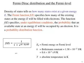
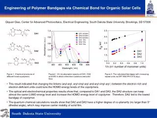
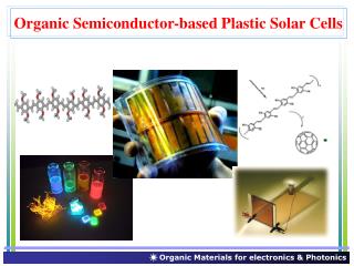
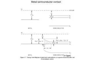
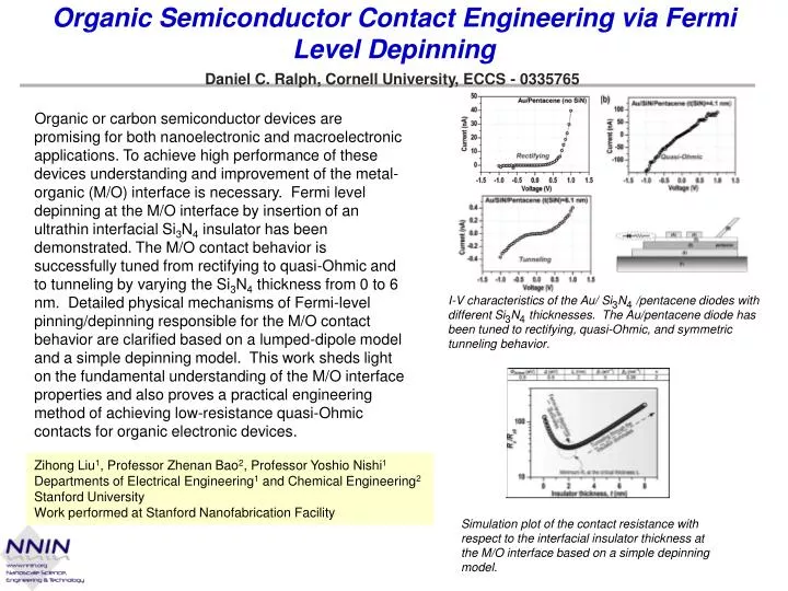
Organic Semiconductor Contact Engineering via Fermi Level Depinning Daniel C. Ralph, Cornell University, ECCS - 0335765 Organic or carbon semiconductor devices are promising for both nanoelectronic and macroelectronic applications.To achieve high performance of these devices understanding andimprovement of the metal-organic (M/O) interface is necessary. Fermileveldepinning at the M/O interface by insertion of an ultrathin interfacial Si3N4 insulator has been demonstrated. The M/Ocontact behavior is successfully tuned from rectifying to quasi-Ohmic and to tunneling by varying the Si3N4thickness from 0 to 6 nm. Detailed physical mechanisms of Fermi-level pinning/depinning responsible for theM/O contact behavior are clarified based on a lumped-dipole model and a simple depinning model. This worksheds light on the fundamental understanding of the M/O interface properties and also proves a practicalengineering method of achieving low-resistance quasi-Ohmic contacts for organic electronic devices. I-V characteristics of the Au/ Si3N4 /pentacene diodeswith different Si3N4 thicknesses. The Au/pentacene diodehas been tuned to rectifying, quasi-Ohmic, and symmetrictunneling behavior. Zihong Liu1, Professor Zhenan Bao2, Professor Yoshio Nishi1 Departments of Electrical Engineering1 and Chemical Engineering2 Stanford University Work performed at Stanford Nanofabrication Facility Simulation plot of the contact resistance with respect to the interfacial insulator thickness at the M/O interface based on a simple depinning model.