Download
1 / 62
620 likes | 628 Views
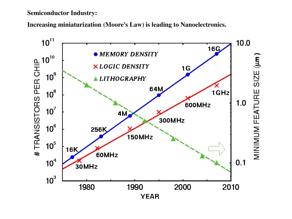
Semiconductor Industry: Increasing miniaturization (Moore’s Law) is leading to Nanoelectronics. Semiconductors: 1. Crystal Properties. (a). (b).

E N D
Semiconductor Industry: Increasing miniaturization (Moore’s Law) is leading to Nanoelectronics.
Semiconductors: 1. Crystal Properties (a) (b) Fig. 1 Relation of the external form of crystals to the form of the elementary building blocks. The building blocks are identical in (a) and (b), but different crystal faces are developed. (c) Cleaving of a crystal of rocksalt. (Introduction to Solid State Physics, Kittel, 7th Ed., John Wiley & Sons, Inc., 1996) (c) Translation Vector: T = u1a1+u2a2+u3a3 Primitive translation vectors: a1, a2, a3 Basis: Composed of at least one atom Rj=xja1+yja2+zja3 0xj, yj, zj 1 Lattice + Basis Crystal Structure Fig. 2 2D Protein crystal, Ibid.
Choices for primitive translation vectors and primitive unit cells which have equal area (cells 1-3). Note cell #4 is not primitive. a1 a2 Primitive cell in 3D Basis with 2 atoms.
The body-centered cubic (bcc) lattice. The primitive translation vectors are a1 = a/2(1,1,-1), a2 = a/2(-1,1,1) and a3 = a/2(1,-1,1) bcc fcc The face-centered cubic (fcc) lattice. The primitive translation vectors are a1 = a/2(1,1,0), a2 = a/2(0,1,1) and a3 = a/2(1,0,1)
Crystal Structure of diamond (C, Si, Ge, Sn) Atomic positions in the cubic cell projected on a face The positions of the atoms can easily be understood from this picture. The white spheres correspond to atomic positions on one fcc lattice, while the black spheres correspond to atoms on the second fcc lattice. The diamond structure can be described as two interpenetrating fcc lattices whose second lattice is displaced along the body diagonal by ¼ of its length. That is, the fcc space lattice consists of a basis with two identical atoms at (000) and (¼ ¼ ¼).
The Zinc-Blende crystal structure. The structure is very similar to the diamond structure except the second fcc lattice consists of a different type of atom. This is a very common crystal structure for binary semiconductor structures shown in the table below: Material a (Å) GaAs 5.65 ZnSe 5.65 AlAs 5.66 ZnS 5.41 AlP 5.45 GaP 5.45 InSb 6.46
IA VIII IIA IIIB IVB VB VIB VIIB
Index system for crystal planes The plane intercepts the a1, a2, a3 axes at 3a1, 2a2, 2a3. The reciprocals of these numbers are 1/3, ½, ½. The smallest three integers having the same ration are 2, 3, 3, thus the indices of the plane are (233). Indices of important planes in a cubic crystal.
Reciprocal Lattice Vectors: G = v1b1+v2b2+v3b3 v1, v2, v3 are integers. We want to describe periodic properties of the crystal using reciprocal lattice vectors and Fourier analysis. For example, take the electron density function n(r). 3-D: 1-D:
Brillouin Zone Construction 1-D 1st Brillouin Zone: Wigner-Seitz primitive cell in the reciprocal lattice. 2-D
Important Brillouin Zones in 3D for fcc and bcc bcc fcc The face-centered cubic (fcc) lattice. The primitive translation vectors are a1 = a/2(1,1,0), a2 = a/2(0,1,1) and a3 = a/2(1,0,1) b1=2/a(-1,1,1), b2=2/a(1,-1,1), and b3=2/a(1,1,-1)
Special points in the fcc and bcc Brillouin zones bcc fcc Special points: X=(0,1,0)2/a, L=(1/2,1/2,1/2) 2/a, K=(3/4,3/4,0)2/a, W=(1/2,1,0) 2/a, U=(1/4,1,1/4)2/a
Free Electron Gas in metals: Example: Electronic Configuration of Na (Sodium) 1s22s22p63s1 Core: 1s22s22p6 Valence: 3s1 Nucleus eZa Core electrons -e(Za-Z) -eZ Valence electrons Za = atomic number Drude Assumption: eZa eZa eZa -neZ valence electrons -e(Za-Z) -e(Za-Z) -e(Za-Z) eZa eZa eZa -e(Za-Z) -e(Za-Z) -e(Za-Z)
Quantum Theory of free electron gas: 1D metal 1D Shrodinger Equation: V(x) Inside metal Outside metal (1) 0 L (x) = Asin(knx); knL=n and kn = 2/n Also Now suppose we have N electrons in a 1D metal. Each k-state can have spin-up and spin-down electrons; ms = ½. Define Fermi Energy as the Energy of the highest filled level: nF = N/2. So n =3 n =2 V(x) n =1 0 L
Another approach for 1D, 2D and 3D electron gas: Solution to Eq. (1) can also be written as (x) = Aexp(ikx) Suppose we have a ring of N atoms with length L. Use periodic boundary conditions: (Also known as Born Von Karman boundary conditions.) (0) = (L) kL=2n and k=2n/L For 3D, the Hamiltonian is L=Na a x X=0,L and
Suppose we have a box with sides a, b, and c (i.e., V=abc) • Then periodic boundary conditions (a,0,0) = (0,0,0) , (b,0,0) = (0,0,0) , and • (c,0,0) = (0,0,0). • kxa=2l, kyb=2m, andkzc=2pwhere l, m, p are 0, 1, 2 ,3 … p It’s possible to construct a “state-space”: pml = n Number of states with a given spin in volume n So m l Since the actual number of states is twice that for a give spin, it follows that kz The volume of the shell is ky It is customary to assume a spherical approximation in k-space: d3k=4k2dk kx
Density of States: Important concept for metals, semiconductors 1D, 2D and 3D. Number of states in the range kk+dk (assuming spherical symmetry) Therefore
Also, for metals we can express the density of states in terms of the Fermi Energy: kz ky For Semiconductors, vary often the surfaces of constant energy aren’t spherical, but rather ellipsoidal. Typically, kx kF Fermi Surface at EF a,b,and c are the axes of the ellipsoid. mxx,myy, and mzz are the effective masses Surface of constant E kz ky b a c kx
In the parabolic approximation of bands, the effective mass depends generally on direction as is defined as: E Eo The volume of the ellipsoid in k-space is kx Remember, (Simple Taylor expansion)
If we define m*=(mxxmyymzz)1/3, then At this point, it’s necessary to introduce the Fermi-Dirac distribution, f(E). So far we have considered a temperature at absolute zero (T=0). f(E) gives the probability that an orbital (or state) will be occupied at energy E for a given temperature T. is the chemical potential and is need for the conservation of electrons in the system. kB is Boltzmann’s constant, at kBT1/40 eV at T=300K. Example: Consider plot of f(E) vs. E/kB for EF=4.2 eV (at T=0) and TF=EF/kB=50,000 K. f(E) f(E) 1 0 T=0, =EF, ,f=1/2 EF E E/kB
The number of electrons between E and E+dE is g(E) T = 0 Also, note here that the density of states depends on the dimension of the system: T > 0 Ntotal E1/2 Const E-1/2 EF E g(E) E
Understanding Bands from the molecular orbital (MO) point of view. A B A B MO2=1sA-1sB =1s* HA HB A B Consider the H2 molecule MO1=1sA+1sB =1s 1s* Antibonding level Antibonding MO E Bonding level V(r) Bonding MO 1s When two atoms are brought together, a higher energy anti-bonding orbital (*) and a lower energy bonding orbital () form which are linear combinations of atomic orbitals (LCAO), as shown above. H2 is the simplest example of this effect. If instead of two atoms, we bring N atoms together, there will be N distinct LCAO and N closely spaced energy levels that will form a band.
Consider two Na atoms in a crystal. The spatial extent of the radial wavefunctions, r(r), is shown below. Notice that there is appreciable overlap only for the 3s valence electrons. Core electrons have significantly reduced overlap. 1s # of nodes =n-l-1 2p 3s NaA NaB 3.7 Å 2s
Tight-binding method for determination of the band sructure: We want to calculate the electronic band dispersion for crystals in which the electron wavefunctions are not significantly different from the atomic case, i.e., they are still tightly bound to the atom. This method is referred to as the tight-binding approximation. Energy levels V(r) r (spacing) -1 Bands form each with N values of k; the bandwidth depends on the overlap of the wavefunctions. n=3 n=2 n=1 d d d d N-fold degenerate levels When d is large: Hatn=Enn, where Hat is the Hamiltonian for an isolated atom, n are the atomic wavefunctions, En are the energy eigenvalues.
Let H = Hat +U(r), where U(r)contains all corrections to the atomic potential required to produce the full periodic crystal potential. r(r) U(r) When U(r)is added to a single atomic potential localized at the origin, the full periodic crystal potential, U(r),is recovered. (r) is an atomic wavefunction, localized at the origin. When |r(r)| large, |U(r)|is small, and vice versa. So, with U(r) = Vat(r) + U(r), and U(r+T)= U(r), An important property of wavefunctions n(r) in crystals is provided by Bloch’s Theorem:
For N atoms, we want to construct linear combinations of the form: where the periodic boundary conditions (i.e. kxLx=2n) are satisfied. Test Bloch conditions: thereby satisfying the Bloch condition. There is a problem with this assumption, however, since negligible overlap of adjacent atomic wavefunctions from site to site would be found for most states. This would lead to very little or no dispersion in the energy bands, inconsistent with the experimental evidence. We want to maintain the general form of the Block solution, but introduce new atomic-like functions (r). where (r) is called a Wannier function. This is expected to be similar to atomic wave functions, so we can expand in terms of the the orthonormal set of bound atomic wavefunctions. (1) (2) LCAO (Linear combination of atomic orbitals)
from the Crystal Hamiltonian (3) Multiply by m*(r) and integrate: (3) (4) Now insert Wannier functions, by putting (1) and (2) into (4) Simplify by considering T=0 terms and (5)
It’s important to note that the overlap is usually small in the tight binding approximation so that For our localized atomic levels: Now, let n run over these levels with energies that are degenerate or very close to a fixed atomic level: s, p, or d level. s-level 1-equation with one unknown energy dispersion E(k). p-level3 equations, 3 energy dispersions Ei(k) d-level 5 equations, 5 energy dispersions Ei(k) As an example, consider single atomic s-level (simplest) case: where bs=1 Then Eq. (5) becomes (6)
Make some definitions: Let We can rewrite (6) as (7) There are symmetry arguments to consider for an s-level: i. (r) is real and (r)=(r) (-T)= (T) ii. Inversion symmetry U(-r) = U(r) and (-T)= (T) iii. Also, <<1 (Small Overlap for adjacent atomic sites) This simplification gives:
Consider fcc lattice with 12 nearest neighbors: T = a/2(±1, ±1,0), a/2(0, ±1, ±1), a/2(±1,0, ±1) Then Also, U(r) = U(x,y,z) has the full cubic symmetry of the lattice and is unchanged by permutations of its arguments or signs. Therefore (T) = const. = Therefore, we can simplify further: using cos(A+B)=cosAcosB-sinAsinB and where is given by
An important characteristic of the tight-binding energy bands: Bandwidth (spread between the maximum and minimum energy) is proportional to the small overlap integral . As the overlap decreases also || decreases. It is therefore clear as 0, E(k) const., forming N-fold degenerate levels. Consider now ka<<1, kx=ky=kz, E(k) =Es- - 12 + k2a2 = Eo + k2a2 E(k) Eo Appears similar to free electron case, i.e. kx Note: kx=ky=kz [111] direction For this tight-binding example:
Consider plot for full zone along the X-direction [100]: E Eo+16 Eo 0 kx 2/a Bandwidth = 16 X [100] Extend the tight-binding method for p-levels, i..e. i=xf(r), yf(r), and zf(r) LCAO involves expressing the wavefunctions as Note: these levels are degenerate. Spherical coordinates and spherical harmonics: Note for l=1 (p-level), ml=-1, 0, 1
(5) For our p-levels: where: and This is a 3 x 3 secular eigenvalue problem for E(k), which, involves 3 eigenvalues and 3 eignevectors from: d-bands involve a 5 x 5 problem, etc.. E1(k) For d-bands, we would calculate 5 bands. In general, we get 3 bands for our p-bands: E E2(k) E 3(k) X kx
Hybridization: LCAO for chemical bonding. For C, Si, Ge, and Sn, the sp3 hybridization describes the covalent chemical bonding in the diamond structure.The mixing of the wavefunctions results in -bond orbitals with the famous 109.5 degree bond angle. The four hybridized wavefunctions are: p sp3 E s Hybridization
Conduction Band States Consider Silicon: 1s22s22p63s23p2 Valence Band States Actual crystal spacing Energy levels in Si a function of the inter-atomic spacing. At the actual atomic spacing of the crystal, the 2N electrons in the 3s sub-shell and the 2N electrons in the 3p sub-shell undergo sp3 hybridization, and at T=0 all 4N electrons end up in the lower 4N states forming the valence bands. The higher lying 4N states form the conduction band, and are empty at T=0. Note that there is a band gap separating the valence and conduction bands.
Energy Bands: T = 0 No sharp distinction between semiconductors and insulators; the energy gap for semiconductors is usually less than ~2eV. E Eg EF Semiconductor, Insulator Metal The bands of a metal are always partially filled. Semiconductors require thermal excitation across the gap to populate conduction levels. E Eg T > 0 Semiconductor, Insulator Metal
Semiconductor or Insulator: Metal: T=0 E Unoccupied states E ECConduction band minimum (CBM) or EF Eg or EF Chemical potential or Fermi level EV Valence Band maximum (VBM) Occupied states Occupied states g(E) g(E) For T > 0, electrons will be thermally excited from the VBM to the CBM. Conduction can only take place when there are carriers (electrons or holes) in partially filled bands. We shall see that the fraction of electrons excited across the band gap (Eg) is proportional exp(- Eg/2kT). For Eg=4 eV the fraction is ~10-35 at T = 300 K (kT=1/40 eV). For Eg=0.25 eV the fraction is ~10-2 at T = 300 K (kT=1/40 eV). Eg is the magnitude of the Band Gap. T > 0 E Unoccupied states Electrons near CBM ECConduction band minimum (CBM) Eg or EF EV Valence Band maximum (VBM) Holes near VBM Occupied states g(E)
Metals vs semiconductors: Transport properties: F= ma =mdv/dt = -eE v = -eEt/m if v(0) = 0. If there is scattering with phonons or impurities, then there is a characteristic collision time , whereby the velocity saturates at vd = -eE/m, where vd is the carrier drift velocity. j = nqvd =ne2E/m=neE(Ohm’s Law) =E = E/ = ne2 /m and = 1/ Also, vd = E by definition. So =e /m (mobility). For metals the scattering rate increases with Temp. (T) so that For semiconductors, the carrier excitation across the band gap is the dominant effect in determining the resistivity () vs T behavior. The basic result is that increases dramatically with T, as we shall see quantitatively. a Log() Typical Metal b = 1/ NDa < NDb Doping 1/T 1/T
Consider briefly optical properties of semiconductors: Indirect Bandgap Direct Bandgap EC EV EC EV E k kc = photon energy Consider the emission of a phonon: = phonon energy = phonon energy (For a direct band gap semiconductor) (For an indirect band gap) (kc= electron momentum) = photon energy Indirect transitions: Almost all the energy is provided by the photon, while almost all the momentum transfer is provided by the phonon in an indirect transition process.
The hole behaves like a particle with positive mass and positive charge. Also, ideally in the valence band at T=0, Holes in semiconductors: EC EV E k X kh ke ke=-kh When one electron is missing at ke, we have ke Construct diagram to illustrate hole dynamics: A hole is an alternate description of a band with one missing electron. The diagram construction gives kh Eh(kh) = -Ee(ke) k The charge of a hole is +e. ke qh = -qe= +e
e ve je The motion of electrons in the conduction band and holes in the valence band under the influence of an electric field is summarized by this sketch. j=qv E vh jh h Equations of motion: Symmetry of the crystal M is real and symmetric, and we can always find a set of orthogonal principal axes such that Details of the band structure: Electrons: Holes:
Consider band structure of Si, Ge, GaAs: For GaAs, CBM is at k=0 (i.e. direct bandgap) me E Consider spin-orbit interactions for the p-like hole bands. We need to consider addition of angular momentum for orbit and spin: J = L + S with L = 1 S = 1/2 j = 3/2 and 1/2 For j=3/2, mj = 3/2 and 1/2 s-like Eg k Heavy Holes (hh) mhh mlh Light Holes p-like mhh mlh For j=1/2 mj = 1/2 (split-off) msoh Split-off holes s-like Curvature
For the conduction band, must consider the dispersion near CBM in k-space: See surfaces of constant energy for the conduction bands. Transverse (T) and longitudnal (L) effective masses (see also the table). For Si, ko 0.85 (--X) where X is at (0,1,0)2/a, For Ge, ko is at the L point which is (1,1,1)/a Note again defines the point (0,0,0). Determine the number of carriers in thermal equilibrium: Essential to know the carrier density as a function of temperature: Ec (T) Ev Definitions: nc(T) = Number of electrons/vol. in conduction band pv(T) = Number of holes/vol. in the valence band gc(E) = Density of states (DOS) in the conduction band gv(E)=DOS in the valence band.
Using Fermi-Dirac statistics: Note that the probability of finding a hole is 1-f(E) For most cases of interest we can approximate using Ec->>kBT and -Ev>>kBT, i.e., is near the middle of the gap, or midgap. Therefore, for E > Ec and E< Ev (E > Ec) (E< Ev) This is the Boltzmann limit. Therefore, the above expressions can be written as (1) (2)
Further define: The DOS for electrons in the conduction band and holes in the valence band is After integration: (3) (4) We can also reduce to a numerically convenient form: Therefore, for mc,vme, the upper limit to the carrier concentration is 1018 to 1019 cm-3 for a non-degenerate semiconductor.
We can eliminate altogether multiplying Eqs. (3) and (4): This is a very useful formula known as “the law of mass action.” Consider now the intrinsic case in which all electrons in the conduction band and holes in the valence band come from thermal excitation. In the intrinsic case, impurities don’t contribute to the conductivity. In the intrinsic case, nc=pv=ni Also nc=pv=ni i = (intrinsic case)
We can express i in terms of the masses: So, as T0, i Eg/2 Even at room temperature kBT 1/40 eV and for Si, Eg ~1.1 eV so i Eg/2 Notes for calculations: (mc)3/2 Rc(mde)3/2 where Rcis the number of equivalent minima and mde is the DOS effective mass for electrons: Also (mv)3/2(mdh)3/2 = mhh3/2 + mlh3/2, where mdh is the DOS effective mass for holes. These masses can be found in standard tables. For semiconductors, the addition of impurities to the crystal will significantly alter the carrier density and conductivity. Donors will add electrons to the conduction band. Acceptors will add holes to the valence band.
Consider a group V impurity donor, e.g. As or Sb (s2p3) in Si or Ge (group IV with sp3) In order to preserve the tetrahedral bonding and symmetry, the extra electron is weakly bound to the impurity donor. e- Si Si Si Coulomb potential Si Sb Si Sb + Behaves like hydrogen atom Si Si Si Four sp3 hybrid bonds are formed, leaving one electron in a hydrogen-like orbit around the Sb. Complete removal of the electron will ionize the Sb donor. Thus, we have a Coulomb force binding the electron as in the hydrogen atom. We have solved this problem in quantum mechanics: n is the principal quantum number, 1, 2, 3, .. (fine structure constant)
The binding energy is given by EB = ET() – ET(n=1) The Bohr radius ro for the impurity can also be easily written: Where ao is the Bohr radius for atomic hydrogen: Example, typically m*0.1me and 10, so EB = 13.6eV(0.1/100) = 13.6 meV Also ro= 0.53Å(10/0.1) = 53Å III IV V B C N Al Si P Ga Ge As In Sn Sb A similar argument can be applied to group III acceptors (s2p): Again, this is a hydrogen-like problem except that the fixed charge is negative and the orbiting charge is a positively charged hole. _ h+ Check the table which list the binding energies for III acceptors and V donors. It is much easier to excite electrons and holes from impurity levels than to excite electrons across the bandgap (intrinsic case). i) Electrons are excited from ED to EC. ii) Holes are excited from EA to EV. (Also equivalent to filling bound hole with e- promoted from the VBM.) EC ED EA EV
The statistics for the donors and acceptors are where ND+ is the number of ionized donors, g = 2 (ground state degeneracy of the donor which can have spin up, down, or no electron). where NA- is the number of ionized acceptors, g = 4 since we have spin up/down and two degenerate valence bands which lead to mj = 3/2 and 1/2 (T) will adjust to maintain charge neutrality: Negative charge = Positive charge For an n-type material (i.e., mostly donors) n = ND+ + p For a p-type material (i.e., mostly acceptors) p = NA- + n, where n = # of electrons in the conduction band and p = # of holes in the valence band. For the partially compensated case: ND+ + p = NA- + n, where both dopants are present.