Download
1 / 58
580 likes | 772 Views
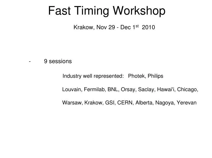
Fast Timing Workshop Krakow, Nov 29 - Dec 1 st 2010. - 9 sessions Industry well represented: Photek, Philips Louvain, Fermilab, BNL, Orsay, Saclay, Hawai'i, Chicago, Warsaw, Krakow, GSI, CERN, Alberta, Nagoya, Yerevan. The Workshop topics (P. Le Du). Photodetectors

E N D
Fast Timing WorkshopKrakow, Nov 29 - Dec 1st 2010 - 9 sessions Industry well represented: Photek, Philips Louvain, Fermilab, BNL, Orsay, Saclay, Hawai'i, Chicago, Warsaw, Krakow, GSI, CERN, Alberta, Nagoya, Yerevan
The Workshop topics (P. Le Du) Photodetectors InitiallyMCP’s Development of large MCP’s (LAPD project) But itisinterestingthis time to heard about timing performance of solid state deviceslike MPPC/SiPM. Electronics , Read out and Trigger FastDigitizers (10-25 psec) Sampling ASIC,TDC … System aspect when large number of pixellatedchannels Improvment of Time Of Flight (TOF) technique Application in multidiciplinaryenvironment HEP , NP and Astro (1 to 50 psec) LHC forwardphysics, new b Factories,Muons, neutrino, FAIR, future SLHC, ILC/CLIC Medical Imaging ( 50-250 psec) TOF-PET, Real Time PET for Hadron-therapy…..
Last IEEE NSS-MIC highlights (Knoxville,TN) - Nov 2010 Progress in scintillators see Paul Lecoq and Marek Moszynskitalks Photodetectors (3 sessions) a SiPM/MPPC/APD array festival A lot of industrialdevelopment Electronics Not much compare to the Clermont workshop Applications Si-PET & TOF-PET
PhotekJ. Howorth, T. Conneely (U Leicester) Next generation photomultipliers - History - (TV idea 1907... 1st PMT: 1934, S1, Tele-movies 1936) - 1945 Sommer: 1st high gain PMT, RCA, EEV 1953 - RCA sold technology to Hamamatsu - MCPs Idea: 1930 Farnworth First: 1960 Oschepkov
Diamond at Photek Diamondfast due to strong band bending (high E field) Collaboration with Bristol Uni; STFC (Rutherford); AWE; Leicester Uni & Photekstarted 2009 Gain from Bristol materialis as good/ betterthan US Operational life testing shows good gain stability and little cathode damage Micro machined parts to 50µm being made Plans for 20µm for nextstep
Multi-anode and Imaging pico-seconddevelopment (T. Conneely) Electronics CERN - Nino ampli/discri: TOT concept, LVDS like output, jitter10ps Max rate 10 MHz - HPTDC: 32 channelat 100ps binning 8 channelsat 25ps
Multi-anode and Imaging pico-seconddevelopment (T. Conneely)3-micron MCPs tube - 8 x 8 multi-anode, 16 x 16 mm2 active area - Two 3-micron pores MCPs - 8 x 8 capacitivelycoupled pads - Fast analogue electronics → highevent rates Read with Nino/HPTDC - Nino board Results: 78ps – 65 ps (delaygeneratorjitter) = 43 ps includeslaser jitter(40 psduration)
Warsaw University of Technology GaAs and Low Temperature Grown GaAs Ultrafast photodetectorsKrzysztof Świtkowski Neutron Irradiated bulk GaAs has a short carrier lifetime comparable with LTG GaAs. Poor electrical properties (especially the resistivity) might rule out it from practical device application (it turns into high dark current and not sufficient sensitivity) Neutron irradiation should decrease carrier lifetime of LTG GaAs and it is very likely that good electrical properties will not be sacrificed Nitrogen implantation of LTG GaAs (I have already received implanted samples from ITME Polish institute of electronic materials technology ) Bi+ and Sb+ implantation might shifts the band-gap of LTG GaAs towards 0.8 eV (anticrossing valance band model) 10
The single electron project, S.White, BNL - ATF beamis 3 picosecbunchlength, exploited to evaluatefast timing detectors? - Common technique for secondarybeam design is successive dispersion and collimation - Single 100 MeV electronscatteredat 90deg into a 1cm2 detector at 30cm - Deepdiffused APD to reject background noise: 650 psrise-time, Al targetchanged for Be, betterresults - DAQ: Waveformsamplingwith scope and DRS4 - Growinginterest in Nuclear and HEP in timing detectors with ~10 ps time resolution. ie extension of pid to new kinematicregion in PHENIX - Pileup rejection at the LHC in forwardphysics (LHC bunch interaction rms=170 ps) - New progress in timing possible similar to Si tracking of last 20 years 12
The single electron project, S.White, BNL Driver for faster timing @LHC is leading protons @L=10^34 Look for new technologies that survive full Luminosity. Hamamatsu (M. Suyama) provided a new device for evaluation. Lifetime tests show >250 Coulomb/cm2 (cp. MCP, 20%loss @0.1Coulomb). 13
The single electron project, S.White, BNL Shannon-Nyquist Reconstruction: Waveform sampling at 2 x max(spectrum), Interpolate with sinc filters, derive intersect to zero 14
Amur Margaryan, Yerevan 17
Amur Margaryan, Yerevan GASTOF with Radio Frequency Phototube Intrinsic Time resolution few ps Rate 10 MHz Stability < 1 ps/hrs Ability to detect several ten events in a ns period 19
Eric Ramberg Fermilab’s Photodetector Timing Program The experimental method Lab measurements of Photek MCP’s Beam tests of Photek with quartz bar radiators Lab measurements of Hamamatsu and IRST SiPM’s Beam test of Hamamatsu SiPM Electronics development MCPs, SiPMs 20
Eric Ramberg Some bench-test results on Photek 240 MCP Single Photon Timing Resolution has better performance than multi-photon extrapolation would indicate (40ps instead of 100ps extrapolated). 21
Eric Ramberg Fermilab’s Test Beam Facility Best beam for timing studies is Main Injector 120 GeV monoenergetic beam with 7 mm spot size Signal, HV cables and gas delivery Spacious control room MWPC and silicon pixel trackers Three motion tables
Eric Ramberg We tested Hamamatsu (Si-PMTs )with different thicknesses of quartz radiator. ~ 60 p.e. with 30 mm quartz t(Q+SiPM) – t(PMT240) after slew corrections Not corrected for electronics (3.1 ps) and PMT240 (7.7 ps) … Intrinsic resolution of better than 15 ps with 30 mm Quartz.
Eric Ramberg Waveform analysis of MPPC with DRS4 DRS4: 5 GS/s, four input channels, PC readout thru USB port Model: charging and discharging of a capacitor: p(x) = (1 - exp(-x/tau1))*exp(-x/tau2) We then convolute this with scintillator decay function and resolution function • Fit the leading edge with T, tau2 and resolution fixed • Use tangent to the middle of the fit to the leading edge to obtain time stamp (resolution of this method is about 4 psec) • Fit the whole pulse to obtain scint decay time T and discharge time tau2
Eric Ramberg Time resolution with LSO crystals • LSO crystals 2x2x7 mm3. Source: 60Co • Hamamatsu MPPC 3.5x3.5 mm2 • Clipping capacitor 10 pF on output of the MPPC • ORTEC preamplifier 120C Use pulse height analysis to select events from photoelectric peak Time resolution 140 ps
Eric Ramberg Summary • Fermilab has been involved in a long series of timing measurements of various photodetectors and our method, using conventional Ortec electronics, consistently gives <3 psec electronic resolution. • Lab measurements of Photek 240 give superb performance – ~45 ps single photon timing resolution • Studies of quartz bar Cerenkov radiators in the beam show that 15 ps level performance TOF is achievable in a variety of conditions • SiPM studies on the bench show interesting differences in wavelength dependence of timing resolution • DRS4 digitizer gives very good (~8 ps) electronic resolution in our lab measurements. Fitting of entire LSO pulses with a Co-60 source gives 140 ps
Véronique Puill (LAL Orsay) Single Photoelectron timing resolution of SiPMs Goal: SuperB Forward PID SiPMTs from HPK, SensL (Ireland), FBK (Italy) 27
Véronique Puill (LAL Orsay) SiPMs Breakdown voltages 28
Véronique Puill (LAL Orsay) SiPMs Breakdown voltage 29
Véronique Puill (LAL Orsay) SiPMs Gain 30
Véronique Puill (LAL Orsay) SiPMs Single PE Timing resolution 31
Dominique Breton, Jihane Maalmi, Eric Delagnes (LAL Orsay, Saclay) Four talks: Towards picosecond time measurement using fast analog memories - The WaveCatcher module : description and performances. Comparison with high-end standard electronics for MCPPMT characterization (NIM paper) [J. Maalmi]. - New SCA circuits and ongoing developments by IRFU/LAL team [D. Breton for E. Delagnes]. - Developments towards large scale implementation of analog memories for precise time measurement [D. Breton]. - - Using fast analog memories for precise time measurement [D. Breton]. 32
Why Analog Memories ? • Analog memories actually look like perfect candidates for high precision time measurements at high scale: • Like ADCs they catch the signal waveform (this can also be very useful for debug) • There is no need for precise discriminators • TDC is built-in (position in the memory gives the time) • Only the useful information is digitized (vs ADCs) => low power • Any type of digital processing can be used • Only a few samples/hit are necessary => this limits the dead time • Simultaneous write/read operation is feasible, which may further reduces the dead time if necessary • But they have to be carefully designed to reach the necessary level of performance … 1. Maximize dynamic range and minimize signal distorsion. 2. Minimize need for calibrations and off-chip data corrections. 3. Minimize costs (both for development & production): Use of inexpensive pure CMOS technologies (0.8µm then 0.35µm); Use of packaged chips (cheap QFP).
About ADCs … • An ADC converts an instantaneous voltage into digital value. It is characterized by: • Its signal bandwidth • Its sampling frequency • Its number of bits (converted / effective) • Collateral dammages : Their package, consumed power, output data rate ! • The most powerful products on the market: • 8bits => 3GS/s, 1,9 W => 24Gbits/s, • 10 bits => 3GS/s, 3,6 W => 30Gbits/s • 12 bits => 3,6GS/s, 4,1 W => 43,2Gbits/s • 14 bits => 400MS/s, 2,5 W => 5,6Gbits/s => appearance of integratedcircularbuffers (limited by technology) • Big companies are experts => our only potential benefit to design ADCs is to integrate them within more complex circuits • The simplest and least power consuming: ramp ADCs (Wilkinson) but they are slow => not adapted to high counting rates BGA 292 pins 24x1,8Gbits/s
Some ADC boards … (3) XMC-1151: 56 GSPS 8-bit dual ADC for 40G/100G communications systems • The ultimate ! • Pb: different possible paths for data • need for calibration • need for knowledge of which path was used
The WaveCatcher module : description and performances. Comparison with high-end standard electronics for MCPPMT characterization (NIM paper). Jihane Maalmi
Jitter sources • Jitter sources are : • Noise : depends on the bandwidth of the system • converts into jitter with the signal slope • Sampling jitter : due to clock Jitter and to mismatches of elements in the delay chain. => induces dispersion of delay durations 2.1 Random fluctuations : Random Aperture Jitter(RAJ) - Clock Jitter + Delay Line 2.2 Fixed pattern fluctuations : Fixed Pattern Jitter(FPJ) => systematic error in the sampling time => can be corrected thanks to an original method based on a simple 70MHz/1.4Vp-p sinewave (10,000 events => ~ 1.5 min/ch)
Methods to extract time - Preferred: digital CFD vs Chi2 due to simpler digital implementation on FPGAs - Chi2 only 10% better. Very detailed analysis and results by Jihane See slides
Pulses on different channels : CFD method • Source: asynhronous pulse sent to the two channels with cables of different lengths or via a generator with programmable distance. • Time difference between the two pulses extracted by CFD method. • Threshold determined by polynomial interpolation of the neighboring points. Spline, extraction of the baseline, and normalization Threshold interpolation 9.64ps rms Ratio to peak 0.23 Time 0.23 σΔt ~ 10ps rms jitter for each pulse ~ 10/√2 ~ 7 ps ! Other method used: Chi2 algorithm based on reference pulses.
Time measurement results : Example with Δt ~ 0 WaveCatcher V4 : 2 pulses with Tr = Tf = 1.6ns and FWHM = 5ns Distance between pulses : Δt ~ 0 Differential jitter = 4.61ps => sampling jitter ~ 3 ps 4.61ps rms All matrix positions are hit!
Effect of CFD ratio on time precision • WaveCatcher V4 : 2 pulses withTr = Tf = 1.6ns and FWHM = 5ns • Δt ~ 0 ns, - Δt ~ 10ns, - Δt ~ 20 ns Optimum value : corresponds to the maximum slope of the pulse!!
Characterization of 10µm- MCPPMT with the WaveCatcher Board • Comparison with high-end standard electronics (NIM paper).
SLAC test summary Summary of all the test results
Fermilab beam test To test the adequation of 10µm MCPPMTs for time of flight measurements Conditions: ~40pe and low gain (2-3 104) Beam CFD with walk correction Raw CFD measurement
SLAC laser test Same conditions as for Fermilab test: 40pe and low gain (2-3 104) WaveCatcher Board 100Hz Tektronix oscilloscope
Summary of the WaveCatcher performances. • 2 DC-coupled 256-deep channels with 50-Ohm active input impedance • ±1.25V dynamic Range, with full range 16-bit individual tunable offsets • 2 individual pulse generators for test and reflectometry applications. • On-board charge integration calculation. • Bandwidth > 500MHz • Signal/noise ratio: 11.8 bits rms (noise = 650 µV RMS) • Sampling Frequency: 400MS/s to 3.2GS/s • Max consumption on +5V: 0.5A • Absolute time precision in a channel (typical): • without INL calibration: <18ps rms (3.2GS/s) • after INL calibration <10ps rms (3.2GS/s) • Relative time precision between channels: <5ps rms. • Trigger source: software, external, internal, threshold on signals • Acquisition rate (full events) Up to ~1.5 kHz over 2 full channels • Acquisition rate (charge mode) Up to ~40 kHz over 2 channels SiPM multiple photon charge spectrum 1 5
Conclusion • The USB Wave Catcher has become a useful demonstrator for the use of matrix analog memories in the field of ps time measurement. • Lab timing measurements showed a stable single pulse resolution < 10 ps rms • We hope to reach 5ps in the next timing-optimized chip (0.18µm) • The board has been tested with MCPPMT’s for low-jitter light to time conversion • Results confirm previous measurements with 40 photo electrons • CFD and Chi2 algorithm give almost the same time resolution: • Double pulse resolution ~ 23 ps => single pulse resolution ~ 16 ps • Even the simplest CFD algorithm can give a good timing resolution • Single pulse resolution < 18 ps • It can be easily implemented inside an FPGA (our next step) • Bandwidth, sampling frequency and SNR are the three key factors which have to be adequately defined depending on the signals to measure (hard with very short signals) • The memory structure has to be carefully chosen and designed to get a stable INL
New SCA circuits and ongoing developments by IRFU/LAL team. Dominique Breton for Eric Delagnes
NECTAR0/SAMLONG block diagram In SAMLONG Chip