1 / 49

Appendix A Logic Circuits

Appendix A Logic Circuits. Logic circuits. Operate on binary variables that assume one of two distinct values, usually called 0 and 1 Implement functions of logic variables Circuits have inputs and outputs Circuits are implemented using electronic logic gates. Standard logic gate

shasta
Download Presentation

Appendix A Logic Circuits

An Image/Link below is provided (as is) to download presentation Download Policy: Content on the Website is provided to you AS IS for your information and personal use and may not be sold / licensed / shared on other websites without getting consent from its author. Content is provided to you AS IS for your information and personal use only. Download presentation by click this link. While downloading, if for some reason you are not able to download a presentation, the publisher may have deleted the file from their server. During download, if you can't get a presentation, the file might be deleted by the publisher.

E N D

Presentation Transcript


  1. Appendix ALogic Circuits

  2. Logic circuits • Operate on binary variables that assume one of two distinct values, usually called 0 and 1 • Implement functions of logic variables • Circuits have inputs and outputs • Circuits are implemented using electronic logic gates

  3. Standard logic gate symbols

  4. Implementation of the XOR function using AND, OR, and NOT gates

  5. Synthesis of logic functions Synthesis is the process of designing and implementing a logic circuit defined by its functional specification. The expression for f in the previous circuit is said to be in a sum-of-products form, because the OR and AND operations are sometimes called the sum and product functions.

  6. Implementationof a logic function

  7. Proving equivalence of expressions

  8. Rules of binary logic

  9. Minimization of logic expressions As illustrated in the previous example, a logic function can be implemented with circuits of different complexities. It is useful to minimize a logic expression to reduce the cost of the synthesized circuit.

  10. Three-variable Karnaugh maps

  11. Four-variable Karnaugh maps

  12. Using don’t cares

  13. NAND and NOR gates

  14. Equivalence of NAND-NAND and AND-OR networks

  15. Cascading of gates

  16. Representation of logic values by voltage levels

  17. Tri-state buffer

  18. A basic latch implemented with NOR gates

  19. Gated SR latch

  20. Gated SR latch implemented with NAND gates

  21. Gated D latch

  22. Master-slave D flip-flop

  23. A negative-edge-triggered D flip-flop

  24. T flip-flop

  25. JK flip-flop

  26. Master-slave D flip-flop with Preset and Clear

  27. Shift register

  28. Parallel-access shift register

  29. A 3-bit up-counter

  30. A two-input to four-output decoder

  31. A BCD-to-7-segment display decoder

  32. A four-input multiplexer

  33. Multiplexer implementation of a logic function

  34. A block diagram for a PLD

  35. Functional structure of a PLA

  36. A simplified sketch of the previous PLA

  37. An example of a PAL

  38. Inclusion of a flip-flop in a PAL element

  39. Organization of a CPLD

  40. A conceptual block diagram of an FPGA

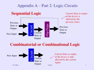
  41. Sequential circuits A logic circuit whose output is determined entirely by its present inputs is called a combinational circuit (e.g. decoders and multiplexers). A logic circuit whose output depends on both the present inputs and the state of the circuit is called a sequential circuit (e.g. counters).

  42. State diagram of a mod-4 up/down counter that detects the count of 2

  43. State table

  44. State assignment table

  45. The next-state expressions are: The output expression is

  46. Implementation of the up/down counter

  47. Timing diagram for the designed counter

  48. A formal model of a finite state machine

More Related