Download
1 / 22
470 likes | 1.05k Views
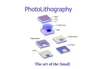
Chapter 5 Lithography. Introduction and application. Light source and photomask, alignment. Photolithography systems. Resolution, depth of focus, modulation transfer function. Other lithography issues: none-flat wafer, standing wave... Photoresist.

E N D
Chapter 5 Lithography Introduction and application. Light source and photomask, alignment. Photolithography systems. Resolution, depth of focus, modulation transfer function. Other lithography issues: none-flat wafer, standing wave... Photoresist. Resist sensitivity, contrast and gray-scale photolithography. Step-by-step process of photolithography. Note: this chapter covers more topics and details than the textbook. But resolution enhancement techniques (phase-shift mask, off-axis illumination…) and advanced lithographies (electron beam lithography…) will not be covered – they will be covered in NE 353 Nanoprobing and lithography. NE 343: Microfabrication and thin film technology Instructor: Bo Cui, ECE, University of Waterloo; http://ece.uwaterloo.ca/~bcui/ Textbook: Silicon VLSI Technology by Plummer, Deal and Griffin
History • Historically, lithography is a type of printing technology that is based on the chemical repellence of oil and water. • Photo-litho-graphy: latin: light-stone-writing. • In 1826, Joseph NicephoreNiepce in Chalon France takes the first photograph using bitumen of Judea on a pewter plate, developed using oil of lavender and mineral spirits. • In 1935 Louis Minsk of Eastman Kodak developed the first negative photoresist. • In 1940 Otto Suess developed the first positive photoresist. • In 1954, Louis Plambeck, Jr., of Du Pont, develops the Dycryl polymeric letterpress plate. Lithography press for printing maps in Munich Lithography stone and mirror-image print of a map of Munich.
Lithography for art: the print principle • Lithography is a printing process that uses chemical processes to create an image. • For instance, the positive part of an image would be a hydrophobic chemical, while the negative image would be water. • Thus, when the plate is introduced to a compatible ink and water mixture, the ink will adhere to the positive image and the water will clean the negative image.
Photolithography for IC manufacturing • In IC manufacturing, lithography is the single most important technology. • 35% of wafer manufacturing costs comes from lithography. • The SIA roadmap is driven by the desire to continue scaling device feature sizes. • 0.7 linear dimension shrink every 3 yr. • Placement/alignment accuracy 1/3 of feature size. Figure 5.2 Patterning process consists of: Mask design Mask fabrication Wafer exposure Figure 5.1
Chapter 5 Lithography Introduction and application. Light source and photomask, alignment. Photolithography systems. Resolution, depth of focus, modulation transfer function. Other lithography issues: none-flat wafer, standing wave... Photoresist. Resist sensitivity, contrast and gray-scale photolithography. Step-by-step process of photolithography. NE 343 Microfabrication and thin film technology Instructor: Bo Cui, ECE, University of Waterloo Textbook: Silicon VLSI Technology by Plummer, Deal and Griffin
Light source: mercury arc lamp Traditionally Hg vapor lamps have been used which generate many spectral lines from a high intensity plasma inside a glass lamp. Electrons are excited to higher energy levels by collisions in the plasma, and photons are emitted when the energy is released. (electron effective temperature 40000K in a plasma!! ) g line =436 nm i line =365 nm (used for 0.5μm and 0.35μm lithography generation) High pressure Hg-vapor lamps Order $1000, lasts 1000 hours. • Filters can be used to limit exposure wavelengths. • Intensity uniformity has to be better than several % over the collection area. • Needs spectral exposure meter for routine calibration due to aging.
Light source: excimer laser Decreasing feature size (to <0.35m) requires shorter . Brightest sources in deep UV are excimer lasers. • Excimer laser: • In excimer lasers, two elements, e.g. a noble gas and a halogen (from a halogen containing compound), which can react and “bind” together only in the excited state but not in their ground states, are present. • Providing energy will therefore drive the reaction, creating the excimer. • When the excitation energy is removed, the excimer dissociates and releases the energy at the characteristic wavelength. • A pulsed excitation is used to repeat the process. Eximer = Excited dimer Xe* + Cl2 XeCl* + Cl XeCl* XeCl + DUV DUV = deep UV, 308nm for XeCl laser XeCl Xe + Cl Here “*” means excited state KrF = 248 nm (used for 0.25μm lithography generation) ArF = 193 nm (currently used for 45nm node/generation production)
Light sources: summary CD: critical dimension Note: the numbers in the two tables are different, so they must be for different systems
Photomask • Types: • Photographic emulsion on soda lime glass (cheap). • Fe2O3 on soda lime glass (no longer in use?). • Cr on soda lime glass and on quartz glass (most popular). • (Quartz has low thermal expansion coefficient and low absorption of light, but more expensive; needed for deep UV lithography). • Transparency by laser printer, more and more popular for MEMS (resolution down to few m with a 20000 dpi printer, very cheap). • Polarity: • Light-field, mostly clear, drawn feature is opaque. • Dark-field, mostly opaque, drawn feature is clear. • Three potential mask improvements: • Pellicle, antireflective coatings, phase-shift masks. • (we want 100% transmission, no reflection) Light-field photomask
Pellicle on a reticle (IC word for mask) Pellicle film Chrome pattern Frame Reticle The particle on the pellicle surface is outside of optical focal range. Antireflective coatings Pellicle film Chrome pattern Depth of focus Mask material • Pellicle: (used only for IC manufacturing where yield is important) • A thin coating of transparent material similar to Mylar is stretched over a cylindrical frame on either side of the mask. • The frame stands off the membrane at a distance of 1 cm from the surface of the mask. • Purpose of pellicle is to ensure that particle that fall in the mask are kept outside of the focal plane of the optical system.
Photomask (Cr pattern on quartz) fabrication • Laser beam writing: • Similar to photolithography, but use a focused laser beam. • It is a direct-write technique - no mask is needed. • Resolution down to a few 100nm, cheaper than electron-beam writing. (Cr is 100nm thick) Remove the resist.
Photomask fabrication by electron beam lithography quartz 12. Finished
Mask fabrication by photo-reduction (demagnification) Minimum feature size 1-5m This is similar to photography, where image is reduced onto the negative film.
Mask fabrication by photo-reduction The beginning “artwork” is huge (close to 1 meter) that can be made easily by printing, the final photomask is only order 1 inch with m feature size on it.
Mask to wafer alignment • 3 degrees of freedom between mask and wafer: x, y, (angle) • Use alignment marks on mask and wafer to register patterns prior to exposure. • Modern steppers use automatic pattern recognition and alignment systems, which takes 1-5 sec to align and expose. • Normally requires at least two alignment mark sets on opposite sides of wafer or stepped region, and use a split-field microscope to make alignment easier. Alignment mark on wafer created from prior processing step. Alignment mark on mask, open window in Cr through which mark on wafer can be seen. Use vernier for more precise alignment
Alignment problems: thermal expansion Pattern on wafer for alignment Alignment mark on mask ΔTm, ΔTsi = change of mask and wafer temperature. m, si = coefficient of thermal expansion of mask & silicon. For example, for thermal expansion of 2ppm/oC (silicon 2.6, fused silica/quartz 0.5 ppm/oC), assume temperature change of 1oC, then the distance between two features separated by 50mm will change by 2ppm or 100nm, which is too large for IC production but OK for most R&D.
Chapter 5 Lithography Introduction and application. Light source and photomask, alignment. Photolithography systems. Resolution, depth of focus, modulation transfer function. Other lithography issues: none-flat wafer, standing wave... Photoresist. Resist sensitivity, contrast and gray-scale photolithography. Step-by-step process of photolithography. NE 343 Microfabrication and thin film technology Instructor: Bo Cui, ECE, University of Waterloo Textbook: Silicon VLSI Technology by Plummer, Deal and Griffin
Three basic methods of wafer exposure Figure 5.3 Less mask wear /contamination, less resolution (depend on gap). High resolution. But mask wear, defect generation. No mask wear/contamination, mask de-magnified 4 (resist features 4 smaller than mask). Very expensive, mainly used for IC industry. Fast, simple and inexpensive, choice for R&D.
Contact/proximity exposure system (called mask aligner) Hard to maintain contact or constant gap when wafer/mask is not even/flat. Resolution (half-period for grating pattern) is given by: g is gap (=0 for contact), t is resist thickness, and is wavelength. • 4 objectives of optical exposure system • Collect as much of radiation • Uniform radiation over field of exposure • Collimate and shape radiation • Select exposure wavelength
Stepper (step and repeat system) UV light source Shutter Alignment laser Shutter is closed during focus and alignment and removed during wafer exposure Reticle (may contain one or more die in the reticle field) Projection lens (reduces the size of reticle field for presentation to the wafer surface) Single field exposure, includes: focus, align, expose, step, and repeat process Wafer stage controls position of wafer in X, Y, Z, Die-by-die exposure Feature size (typically) 4 reduction
Excimer laser (193 nm ArF ) Illuminator optics Reticle library (SMIF pod interface) Beam line Wafer transport system Reticle stage Wafer stage Auto-alignment system 4:1 Reduction lens Step and scan (stepper) exposure system: 193nm 193nm stepper systems are used today for IC manufacturing. Excimer laser: light is in pulses of 20ns duration at a repetition rate of a few kHz. About 50 pulses are used for each exposure. Optical train for an excimer laser stepper
Step and scan (stepper) exposure system: 157nm However, 157nm was not used for production and will never be used, because it needs expensive vacuum (air absorb 157nm), and lens materials (CaF2) have much higher thermal expansion coefficient than quartz (quartz absorb 157nm, thus unsuitable).