Download
1 / 33
330 likes | 430 Views
Readout Status and Plans. M. Andrew, E. Choi, R. Conrad, S. Dubey , B. Kirby, B. Macek , H. Mehta, K. Nishimura, M. Rosen, X. Shi, L. Wood, G. Varner, G. Visser Feb. 6, 2014 B2GM Update. Executive Summary. Production ASICs in fabrication (~April)

E N D
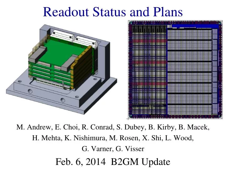
Readout Status and Plans M. Andrew, E. Choi, R. Conrad, S. Dubey, B. Kirby, B. Macek, H. Mehta, K. Nishimura, M. Rosen, X. Shi, L. Wood, G. Varner, G. Visser Feb. 6, 2014 B2GM Update
Executive Summary • Production ASICs in fabrication (~April) • Intermediate board stacks (IRS3C ASIC) almost complete pulser, laser scans planned & then commission on CRT (March) [enough for 3x TOP modules] • Pre-production board stack: • Use same HV, Front board as Intermediate • Master FPGA chosen, SCROD Rev. B in design • Carrier Rev. E – basic layout/amplifier design • Mechanics almost same (no Interconnect board) • Passed Director’s Review, gearing up for CD-2/3
Preliminary answers to BPAC Quantifying effectiveness of timebase feedback (stability)
Preliminary answers to BPAC “Recovering” saturated pulse data and demonstration of the timing thus achieved
Preliminary answers to BPAC Codify a set of ASIC, Carrier, SCROD and full board-stack test/qualification procedures
Reminder: Subdetector Readout Module (a/k/a “the boardstack”) Example IRS Boardstack • IRS ASIC reads out 8 channels • Require 2 ASICs to read out 16 PMT channels • 4 x ASICs per self-contained carrier board (32 channels) • 4 x ASIC carrier boards arranged in compact boardstack (128 channels) • Combined readout electronics, mechanical support and cooling • 4 boardstacks per iTOP module (512 channels) 6
LEPS/SPring-8: 9 PCBs 7 distinct designs (6 UH; 1 IU) IRS3B/spartan6 boardstack versions intermediate: 8 PCBs 6 distinct designs (4 UH; 2 IU) IRS3C/spartan6 pre-production prototype: 7 PCBs 4 distinct designs (2 UH; 2 IU) IRSX/zynq new stuff: thermal walls, AKA spacers SCROD “fake” revB (mockup) SCROD revA3
Intermediate (IRS3C) 1) Assembled board stack 2) Alignment jig plate 3) Angle plates Transition to pogo-pins: need precise assembly jigs (being designed) 8
Intermediate Board Stack • Pogo pins and HVB • Pins: Mill-Max # 0926-1-15-20-75-14-11-0 • Prototype in carriers (HVB & signal types) machined from PEEK • Pin carrier flatness is an issue for assembly • Considering injection-molded carriers, or perhaps mold pins in place (if Mill-Max can do this) • Signal integrity tested for pogo pins: Equivalent to <1.8 nH inductor, which does not limit our signal bandwidth • Basic active divider works very well, vetted in LEPS beam test • Repackage for pogo-pin interconnect and more compact layout • Compact layout requires encapsulation for HV insulation • The encapsulation also provides thermal coupling to a new design cooling bracket compatible with spacer-block clamped boardstack • New HVB board layout in progress. Will be assembled and encapsulated at IU for preliminary tests. • Vendor identified for production encapsulation, quote received.
Intermediate Board Stack • Front board (pogo-pin lands) Front board layout (99% final) Design reviewed 12/2013 To be submitted for fabrication this week • PMT pins are fully buried inside a 4mm thick PCB • Low insertion force pin receptacles contact PMT pins • Pin receptacles are press-fitted to PCB (maximizes HV clearance and cleanliness, and simplifies assembly) • 7-layer sequential lamination (2×), blind via PCB routes anode signals and HV bias to pogo-pin contact pads on rear side • “Arbitrary” pitch and location adaptation between PMT’s and readout boardstack – a challenge, met Mechanical prototype front board (received 11/13/2013) (No routing, no internal layers)
Intermediate Board Stack • Carrier Rev. D (c02, c13)
Intermediate Board Stack • Pulser, laser test stand upgrade
Intermediate Board Stack • Test schedule (gets to Fuji Hall and then onto CRT)
Toward Fuji Hall campaign • Repackaged Sci-Fi (75x, 75y scint fiber – no ribbon cables) 3A @ 5V 1.7A @ -3.3V • 9U KLM readout firmware development (same)
Readout ASIC status:Design completed/reviewed, in fabrication IRS3/X ASIC 50W term • IRS2 ASIC ~8mm Timing Generator Die Photograph • 8 channels per chip @ 2.7-4 GSa/s • Samples stored, 12-bit digitized in groups of 64 • 32k samples per channel (8us at 4GSa/s) • IRS3C* (April 2013) usable for Belle II • Increased performance margin ASICs in fab: • IRSX with high-speed serial interfaces • IRS3D with enhanced dynamic range, same I/O • * IRS3C = IRS3B with low power-on current, ext. dynamic range 15
IRSX • Baseline ASIC for production (800 expected in pre-production run) • High-speed, lower power/EMI LVDS outputs for fast, asynchronous signals • Extended dynamic range comparator • Lower-power Gray Code Counter and internal DLL demonstrated (TARGET7) • IRS3D takes the internal improvements, but keeps IRS3C user I/O 2.6M transistors, 7.7k resistors (DACs)
TSMC Engineering Run • Incremental cost ~zero (reduced risk) IRS3D IRSX TARGETX IRS3C Expect 836 of each (though yield near edge of wafer may be low) We will own the masks, can make rest of production fab with Engr Run Reticle Layout
Pre-production Board Stack • SCROD Rev. B
Pre-production Board Stack • Carrier Rev. E
Pre-production Board Stack • Amplifier and calibration signal path • Two-stage amplifier enables high speed response (600 psrisetime) with low gain operation of PMT • First stage is a load resistor and noninverting voltage amplifier, for better matching to characteristic impedance of the anode signal routing line • Second stage inverts the signal (necessary for IRSX readout polarity) • Calibration signal summed (when enabled) with main signal – no switches in main signal path • Calibration signal bussed across 8 (or possibly 16) channels; switches chosen for minimal loading on disabled channels • 3.5V power supply limits output swing to protect the ASIC against latchup Simplified signal path schematic CAL switch – one possible scheme, now prototyping
Pre-production Board Stack • Amplifier and calibration signal path Typical raw single-pe PMT pulse HVB @ −3200 V 25 Ohm load 20 GS/s (RTO1044) measured risetime: 140 ps 1 mV/div PMT gain ~ 5×10⁵ 1 ns/div Typ. amplified single-pe pulse HVB @ −3200 V Voltage on 10 pF load (IRSX eq.) 20 GS/s (RTO1044) Measured risetime: 565 ps [NOTE: different event & channel] 50 mV/div
8 COPPER High Speed Link Board? 64 DAQ fiber transceivers Waveform sampling ASIC 32 FINESSE 32 FINESSE 8 COPPER UT3 Trigger module 8k channels 1k 8-ch. ASICs 64 SRM “board stacks” Clock jitter cleaners 16 FTSW FTSW clock, trigger, programming 22 64 SRM
Calibration requirements Subtract storage cell pedestal (avg. ~2000 ADC +/- 100’s counts) Linearity correction (optional) Individual sample time offset correction 23
Data Analysis in Hardware • Basic beam test analysis implemented in FPGA • Fully pipelined architecture for maximum performance • Initial measurements: 570k waveforms/sec • Fiber, memory access will reduce max rate; studies underway now • Testbench development for detailed performance analysis with replayed data underway 24
Schedule • Intermediate BS readout of Fuji prototype
Schedule • Pre-production board stack completion
Schedule • Production test procedures and division of labor (@ S. Carolina & Pittsburgh)
Summary • Into the end-game for production • Remaining issues: • Choice of SCROD FPGA (made) • IRSX as baseline (IRS3D, IRS3C as backup) • Confirming pogo-pin interface • Confirming final amplifier configuration • Final power cabling • Intermediate board stacks for validating thermo-mechanics of pre-production designs • Key milestones are: operation in CRT, completing pre-production board-stack, and establishing/validating production testing procedures 28
FTSW, COPPER, CAMAC Picosecond laser Insufficient time/laser scanning resources before LEPS beamtest – subsequent testing in Hawaii Inside Dark Box Dark box too small – being rebuilt Stage for x-y control of illumination fiber (picosecond laser) Module under test w/ reference SL-10 MCP 29
Event sampling • Sampling: 128 (2x 64) separate transfer lanes Recording in one set 64, transferring other (“ping-pong”) • Storage: 64 x 512 (32k per ch.) • Wilkinson ADC (64 at once) • 64 conv/channel (512 in parallel)
Belle II iTOP Counter (3) • A highly constrained cylinder • 3-key elements (1) (2) 31
Readout Electronics -- requirements • Operate within Belle-II Trigger/DAQ environment • >= 30kHz L1 trig • Gbps fiber Tx/Rx • COPPER backend • Timing trigger • iTOP: 8k channels • 16 iTOP modules • 4x 128-channel SRM/iTOP module (64x total) SuperKEKB RF clock 32
Belle II back-end Upgraded for Belle II • COPPER (COmmon Pipelined Platform for Electronics Readout) • Used in Belle, J-PARC experiments • FINESSE (Front-end Instrumentation Entity for Subdetector Specific Electronics) 33