Download
1 / 12
120 likes | 412 Views
Contact Modeling and Analysis of InAs HEMT . Seung Hyun Park, Mehdi Salmani- Jelodar , Hong -Hyun Park, Sebastian Steiger , Michael Povoltsky , Tillmann Kubis , and Gerhard Klimeck Network for Computational Nanotechnology (NCN) Electrical and Computer Engineering Purdue University.

E N D
Contact Modeling and Analysis of InAs HEMT Seung Hyun Park, Mehdi Salmani-Jelodar, Hong-Hyun Park, Sebastian Steiger, Michael Povoltsky, TillmannKubis, and Gerhard Klimeck Network for Computational Nanotechnology (NCN) Electrical and Computer Engineering Purdue University Network for Computational Nanotechnology (NCN)
2015-2019 Research Towards III-V MOSFET • Device geometries • Channel materials • High-k dielectrics and metal gates • Channel doping • S/D doping • Strained-Si channel • High-k dielectrics New Channel Materials Acknowledgement: Robert Chau, Intel Limitation of Si Moderate carrier mobility
Why HEMTs? • III-V: Extraordinary electron transport properties and high injection velocities • HEMTs:Similar structure to MOSFETs except high-κ dielectric layer • Excellent to Test Performancesof III-V material without interface defects • Short Gate Length HEMTs are Introduced by del Alamo’s Group at MIT • Excellent to Test Simulation Models • (SS, DIBL, short channel effects, gate leakage current, scaling, …) • Predict performance of ultra-scaled devices 2008: 30nm 2007: 40nm D.H. Kim et al., EDL 29, 830 (2008)
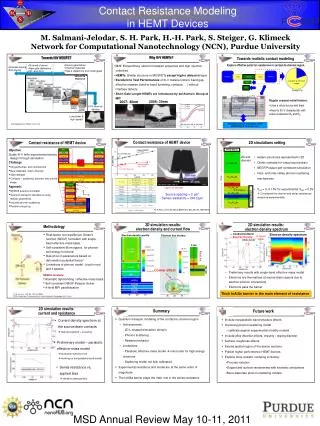
Towards realistic contact modeling Channel region Contact 1 Contact 2 Lead 1 channel Lead 2 Contact-to-channel region channel channel Device Pie • Regular compact model features: • Used Virtual Source and Drain. • Fit I-V characteristic in a post-processing step with series resistances (RS/D) from experimentalist or ITRS. Simulation Domain Simulation domain of compact model (IEDM 2009, N. Kharche et al.)
Modeling Objective / Challenge Objective: • Guide experimental III-V HEMT device design through realistic contact-to-channel region simulation Challenge: • 2-D geometries with multiple materials for hetero structure • Quantum confinement • Effects - scattering, disorder, and curved shape Approach: • Quantum transport simulations in realistic geometries • Include electron-phonon scattering • Parallel computingdue to high computation cost D.-H. Kim, J. D. A. del Alamo, IEEE Trans. Elec. Dev. 57, 1504 (2010) region of interest Contact Pad N+ Cap InGaAs 35nm InAlAs 15 nm Y InP etch stop 6 nm X In0.52Al0.48As 11 nm 2 nm In0.53Ga0.47As InAs 5 nm Virtual Drain 3 nm In0.53Ga0.47As In0.52Al0.48As 13nm
Contact resistance of InAs HEMT device Contact Pad Rpad Question: Where is contact resistance from? N+ Cap InGaAs/InAlAs Rcap Y Contact resistance between the channel and the contact pad. Tunneling resistance from multiple hetero-barriers in HEMT. Current crowding in curved area may cause some resistance. Electron-Phonon scattering. Schottky barrier between contact pad and n-doped cap layer. Alloy disorder and surface roughness. InP etch stop X In0.52Al0.48As Rbarrier In0.53Ga0.47As Rside InAs Virtual Source In0.53Ga0.47As In0.52Al0.48As 1 2 3 are taken into the account are being implemented 4 5
2D Simulations Setting 25nm 2-D hetero structures explicitly represented: Effective masses extraction, band offset, electron affinity, and other parameters Phonon scattering mechanism is included This is essential in this work not only for reasonable resistance value but also for making simulations convergence Extract resistive characteristic from I-V: VDS = 0.5~0.15V for experimental VDD = 0.5V Considered voltage drop from the channel and series resistances measured experimentally Source In53Ga47As 2-D simulation domain In52Al48As 90nm InP In52Al48As Si δ-doping In53Ga47As InAs virtual drain In53Ga47As In52Al48As 40nm
Simulation Approach • Real-space non-equilibrium Green’s function (NEGF) formalism within effective mass approximation • Self-consistent Born approximation for phonon self-energy functions1 • Bulk phonon parameters based on deformation potential theory2 • NEMO5(NanoElectronic Modeling Tool) • Self-consistent NEGF-Poisson Solver for transport calculation • Parallel processing with more than 2000 cores [1] S. Jin et al., JAP 99, 123719 (2006) [2] M. Lundstrom, Fundamentals of carrier transport (Cambridge Univ. Press)
2D simulation results: electron density spectrum --- Conduction Band --- Electron Density δ-doped Layer Electron density spectrum EF InAlAs barrier EF Y δdoped layer Energy (eV) Energy (eV) InAlAs N+ cap Channel Position (nm) EF Position (nm) EF • Preliminary simulation results • Electrons are well-thermalized at source/drain regions due to phonon interactions. • Thick InAlAs barrier is the main element of resistance.
2D simulation results: Resistive characteristic Resistance (Ωμm) Close to experimental result ≈ 240 Ω-μm Voltage (V) D.-H. Kim, J. D. A. del Alamo, IEEE Trans. Elec. Dev. 57, 1504 (2010) • Resistive characteristic (Series resistance vs. Applied bias) • Close to experimental resistance ≈ 270 Ω-μm, but still discrepancy • Preliminary model • Working on non-parabolic effective-mass for improvement • Schottky barrier and other scattering models (surface roughness / alloy disorder) are not yet included.
Summary / Future work • Our First Quantum Transport Model of Contacts in InAs HEMT • Achievements: - 2D L-shaped simulation, phonon scattering, resistive behavior • Limitations: - Current EM model over-predicts the Fermi Level Improve non-parabolic band structure effects • - Phonon scattering model not fully calibrated • Improve calibration against experimental mobility models • Experimental resistance and model are at the same order of magnitude • The InAlAs barrier plays the main role in the series resistance